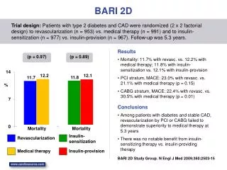
Download
1 / 20
200 likes | 432 Vues
TRD2005,Bari,10.09.05. Progress report on SiPM development and its applications. Boris Dolgoshein Moscow Engineering and Physics Institute. Boris@mail.cern.ch. Single photon Avalance Diodes(SPAD’s): S.Cova et al.,Appl.Opt.35(1996)1956. h . 50 . R 50 .

E N D
TRD2005,Bari,10.09.05 Progress report on SiPM development and its applications Boris Dolgoshein Moscow Engineering and Physics Institute Boris@mail.cern.ch
Single photon Avalance Diodes(SPAD’s): S.Cova et al.,Appl.Opt.35(1996)1956
h 50 R 50 substrate Ubias TWO STEPS IN DEVELOPMENTS OF GEIGER MODE APD: • FIRST STEP: SINGLE PHOTON AVALANCHE DIODE (SPAD), based on single pixel “photon counter” • SECOND STEP: from SPAD to Silicon Photomultiplier (SiPM) • NEXT STEP: Large area SiPM`s from 1x1 mm2> up to 10x10 mm2 46 pixels fired Depletion 1-2m Multipixel (typically ≤ 1 mm2) Geiger mode photodiode with common readout B.Dolgoshein,’Large area SiPM’s…’
SiPM’s have been developed in Russia during last ~10 years(see International Conferences on New Developments in Photodetection ICNDP-1999, 2002,2005) There are four SiPM’s producers for the time being-at the level of test batches production: Center of Perspective Technology and Apparatus CPTA,Moscow MEPhI/Pulsar Enterprise,Moscow JINR(Dubna)/Micron Enterprise HAMAMATSU started the SiPM production last year
42m 20m pixel h Al R 50 Depletion Region 2 m Substrate Ubias SiPM today-reminder: • Pixel size ~20-30mm • Working point: VBias = Vbreakdown + DV ~ 50-60 V • DV ~ 3V above breakdown voltage • Each pixel behaves as a Geiger counter with • Qpixel = DV Cpixel with Cpixel~50fmF Qpixel~150fmC=106e • Electrical inter-pixel cross-talk minimized by: • decoupling quenching resistor for each pixel • boundaries between pixels to decouple them • reduction of sensitive area • and geometrical (packing) efficiency Resistor Rn=400 k -20M Very fast Geiger discharge development < 500 ps Pixel recovery time = (Cpixel Rpixel) ~ 20 ns …1mks Dynamic range ~ number of pixels saturation
3x3mm SiPM parameters • Sensitive area : 3x3 mm2 # of pixels: 5625 • Depletion region: appr. 1 m • Pixel size: 30 mx30 m • Working voltage: 20…25 V Gain: 1…2 x10**6 • Dark rate.room temperature: 20 MHz • SiPM noise(FWHM): • room temperature 5-8 electrons • -50 C 0.4 electrons • Single pixel recovery time: 1us • After pulsing probability: appr. 1% • Optical crosstalk: appr. 30 - 50 % • ENF: appr. 1.5-2.0(overvoltage dependent)
Spectral dependence of the photon detection efficiency (PDE) for different photodetectors • 178nm-5.5%,(1mmx1mm SiPM)
Photon detection efficiency= QE(~80%)x x packing efficiency(active/total area,~40%)x x Geiger efficiency(~70%)
Optical Crosstalk OC • –due to secondary light emitted • in Geiger discharge: 10**-5 photons/one electron • adjacent pixels are fired- fig’s. • OC increases drastically with a Gain • becomes >1 for a Gain > few timesx10**7 selfsustening discharge • pixel independence and Poisson statistics of fired pixels are violated • Excess Noise Factor ENF becomes too large • Secondary light: Effective absorption length(Si)- appr. 50 mkm Effective wavelength- appr. 1000 nm B.Dolgoshein,’Large area SiPM’s…’
Optical crosstalk,SiPM 1x1 mm2,dark noise Crosstalk==>non-Poissonian distribution: pixel fired/phe=1.7 ENF=1.6 Gain 3x10**6 Crosstalk suppression by special SiPM topology: test structure,PRELIMINARY! Poisson distribution: pixel fired/phe= 0.98+-0.03 ENF= 0.97+-0.05 Gain 3x10**7 B.Dolgoshein,’Large area SiPM’s…’
Recovery time of single pixel: C(pix)xR(pix)-->20ns…..a few mks
Temperature and bias voltage dependence: delta T(V) Gain Signal=GainxPDE -1 C +2.2% +4.5% +0.1V +4.3% +7%
Comparison of the SiPM characteristics in magnetic field of B=0Tand B=4T (very prelimenary, DESY March 2004) LED signal ~150 pixels A=f(G, , x) No Magnetic Field dependence at 1% level (Experimental data accuracy)
SiPM signal saturation due to the limited total number of Sipm’s pixels Response functions for the SiPMs with different total pixel numbers measured for 40 ps laser pulses
Long term stability of SiPM • 20 SiPMs worked during 1500 hours • Parameters under control: • One pixel gain • Efficiency of light registration • Cross-talk • Dark rate • Dark current • Saturation curve • Breakdown voltage No changes within experimental errors 5 SiPM were tested 24 hours at increased temperatures of 30, 40, 50, 60, 70, 80, and 90 degrees No changes within experimental accuracy
SiPM long term stability 20 tested SiPMs worked during 1500 hours • Parameters under control: • Efficiency of light registration • One pixel gain • Dark rate • Dark current
SiPM today: - + Low noise,high gain Good single electron resolution Very good timing Small recovery time Very low nuclear counting effect Insensitivity to B Simple calibration and monitoring Vow bias voltage Low power consumption Compactness Room temperature operation Good T and V stability Simplest electronics Relatively low expected cost(low resistivity Si,simple technology) Not very high PDE Small area High dark rate(~ area) Exess Noise Factor is large enough due to Optical Xtalk