Download
1 / 43
430 likes | 472 Vues
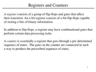
This chapter covers the objectives, study guide, and design of registers and counters, including binary and shift registers, counter design using flip-flops, and derivation of flip-flop input equations. It also features figures and timing diagrams for related concepts.

E N D
This chapter in the book includes: Objectives Study Guide 12.1 Registers and Register Transfers 12.2 Shift Registers 12.3 Design of Binary Counters 12.4 Counters for Other Sequences 12.5 Counter Design Using S-R and J-K Flip-Flops 12.6 Derivation of Flip-Flop Input Equations--Summary Problems FIGURES FORCHAPTER 12REGISTERS AND COUNTERS Click the mouse to move to the next page. Use the ESC key to exit this chapter.
Figure 12-1: 4-Bit D Flip-Flop Registerswith Data, Load, Clear, and Clock Inputs
Figure 12-3: Logic Diagram for 8-Bit Register with Tri-State Output
Figure 12-9: Typical Timing Diagram forShift Register of Figure 12-8
(b) Figure 12-19ab: Loadable Counter with Count Enable
Table 12-3: State Table for Figure 12-21 Figure 12-21: State Graph for Counter
(c) Logic circuit Figure 12-27:Counter of Figure 12-21Using S-R Flip-Flops
Table 12-9. Determination of Flip-Flop Input Equations from Next-State Equations Using Karnaugh Maps
Figure 12-29a:Derivation of Flip-Flop Input EquationsUsing 4-Variable Maps
Figure 12-29b:Derivation of Flip-Flop Input Equations Using 4-Variable Maps
Figure 12-29c:Derivation of Flip-Flop Input Equations Using 4-Variable Maps