Download
1 / 38
380 likes | 517 Vues
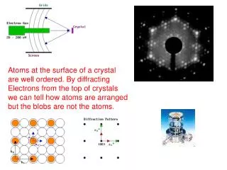
Atoms at the surface of a crystal are well ordered. By diffracting Electrons from the top of crystals we can tell how atoms are arranged but the blobs are not the atoms.

E N D
Atoms at the surface of a crystal are well ordered. By diffracting Electrons from the top of crystals we can tell how atoms are arranged but the blobs are not the atoms.
Atoms were seen for the first time at the end of very sharp needle of tungsten ( 20 atom radius) by applying very high voltage
We can make quantum corals with atoms by moving one atom at a time
It took us a few seconds to write this over an area of 400x400m2 by using Pb atoms on the tip and dropping them off with high voltage pulse
Histogram of height distribution 2000 x 2000 Å growth on Si(111)-(7x7), =3 ML, T=185 K. These STM results confirm earlier diffraction results showing that Pb islands of the same height are grown at low temperature • The discrete energy levels of the confined electrons dictate the film morphology.
The width corresponds to the island height and the wave to the electrons inside the island Electrons inside the islands are like notes on violin “string”. When the notes are “tuned” we have the selected height
Whenever intensity is a maximum. Whenever intensity is a minimum. Diffraction from Thin Films We use a diffraction technique similar to optical diffraction from “air wedges” to determine the island thickness. h
Intensity Oscillations with electron energy similar to optical “fringes” Diffracted intensity oscillations have shown unusual 7-fold periodicity. This corresponds to 7-step islands at 180K For single steps one oscillation would be observed K. Budde, E. Abram, V. Yeh, M.C. Tringides, Phys. Rev. B Rapid Comm. B61 10602 (2000)
Spin polarized spectroscopy with magnetic tips The tunneling current depends on the overlap of the sample tip density of states Both ferromagnetic and anti-ferromagnetic tips can be used because only the last atom determines s the polarized current Magnetic samples have non-zero polarization Only the same sample polarization as the tip is selected by the tunneling process At sufficiently low bias and for polarized tips one is sensitive to spin states in the sample of the same polarity so the spin dependent density of states can be measured M.Bode Rep. Prog. Phys. 66 523 2003)
Magnetic vortex for large enough island ( Larger than 5nm) then not a single domain structure. This is easily seen in dI/dU maps because a different spin polarization is seen when the center is Crossed. Magnetization “curles” around the center.
Mg deposition at 102K, annealed to RT with screw dislocation network 100x100nm2 Tailored bimetelalic islands Co surrounding Pt cores have the same magnetic properties as pure Co islands Rusponi et al. Nat. Mat. 2 (2003) 546 Very preliminary experiments of Fe-Mg coadsorption show the same decoration of the Mg edges by Fe After Fe 0.3ML deposition at RT Fe adsorbs preferably at the terrace edges
An AFM SEM image of the cantilever/probe used in an AFM force sensor (right). SiN is used for creating probes that have very low force constants. The thin films used for creating SiN probesmust have very low stress so the cantilevers don’t bend naturally from the stress. Practically, most SiN films have some residual stress and in fact, cantilevers made with SiN tend to have curvature along their primary axis.
SiN cantilevers are typically triangular with two arms meeting at an apex. The probe on SiN probes are typically pyramidal and appear hollow at the top. (Top) Si cantilevers are typically rectangular and the probes tend to have a triangular shape to them. Si probes are crystalline and are probe to chipping and breaking if they crash into a surface. (Bottom)
Left: A piezoelectric cylinder has electrodes on the inside and outside so that the potential goes through the wall of the ceramic. When activated the cylinder elongates. Right: A piezoelectric 9 Top: PZT materials have hysteresis. When a voltage ramp is placed on the ceramic, the motion is nonlinear. Bottom: Creep occurs when a voltage pulse on a PZT causes initial motion followed by drift.bimorph has two sheet of piezoelectric material bonded together. The end of the bimorph expands in a parabolic motion when activated.
The force between tip and sample is not measured directly, but calculated by measuring the deflection of the lever, and knowing the stiffness of the cantilever.Hook’s law gives F = -kz, where F is the force, k is the stiffness of the lever, and z is the distance the lever is bent.
Contact Mode As the tip is raster-scanned across the surface, it is s deflected as it moves over the surface corrugation. In constant force mode, the tip is constantly adjusted to maintain a constant deflection, and therefore constant height above the surface. Because the tip is in hard contact with the surface, the stiffness of the lever needs to be less that the effective spring constant holding atoms together, which is on the order of 1 - 10 nN/nm. Most contact mode levers have a spring constant of < 1N/m. Lateral Force Microscopy LFM measures frictional forces on a surface. By measuring the “twist” of the cantilever, rather than merely its deflection, one can qualitatively determine areas of higher and lower friction. Noncontact mode Noncontact mode belongs to a family of AC modes, which refers to the use of an oscillating cantilever. A stiff cantilever is oscillated in the attractive regime, meaning that the tip is quite close to the sample, but not Touching it (hence, “noncontact”). The forces between the tip and sample are quite low, on the order of pN (10 -12 N). Dynamic Force / Intermittant-contact / “tapping mode” AFM Commonly referred to as “tapping mode” it is also referred to as intermittent-contact or the more general term Dynamic Force Mode (DFM).A stiff cantilever is oscillated closer to the sample than in noncontact mode. Part of the oscillation extends into the repulsive regime, so the tip intermittently touches or “taps” the surface. Very stiff cantilevers are typically used, as tips can get “stuck” in the water contamination layer.
Force Modulation Force modulation refers to a method used to probe properties of materials through sample/tip interactions. The tip (or sample) is oscillated at a high frequency and pushed into the repulsive regime. The slope of the force-distance curve is measured which is correlated to the sample's elasticity. Phase Imaging In Phase mode imaging, the phase shift of the oscillating cantilever relative to the driving signal is measured. This phase shift can be correlated with specific material properties that effect the tip/sample interaction. The phase shift can be used to differentiate areas on a sample with such differing properties as friction, adhesion, and viscoelasticity.
The forces applied to the surface by the probe in contact mode are given by Hook's law: Left: Potential diagram showing the region of the probe while scanning in contact mode. Right: In contact mode the probe glides over the surface.
Left: Potential diagram showing the motion of the probe in vibrating mode. Right: The probe vibrates as it scans across a surface.
imaged with the atomic force microscope (AFM) in contact mode
SNOM image of latex nanospheres separated by 40nm
Most AFMs use a laser beam deflection system. A laser is reflected from the back of the reflective AFM lever and onto a position-sensitive detector. AFM tips and cantilevers are microfabricated from Si or Si3N4. Typical tip radius is from a few to 10s of nm.