Class B Output
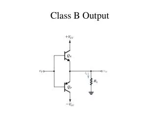
Class B Output. Biasing the Class B Output. * No DC current is used to bias this configuration. *Activated when the input voltage is greater than the Vbe for the transistors. * npn Transistor operates when positive, pnp when negative. * At a zero input voltage, we get no output voltage.

Class B Output
E N D
Presentation Transcript
Biasing the Class B Output * No DC current is used to bias this configuration. *Activated when the input voltage is greater than the Vbe for the transistors. * npn Transistor operates when positive, pnp when negative. * At a zero input voltage, we get no output voltage.
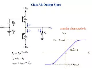
Operation When the input voltage rises to be large enough to overcome the Vbe, it will begin to cause an output voltage to appear. This occurs because Qn begins to act like an emitter follower and Qp shuts off. The input will be followed on the emitter until the transistor reaches saturation. The maximum input voltage is equal to the following: The same thing will begin to happen if the input voltage is negative by more than the Veb of the transistor. This causes the Qp to act like an emitter follower and Qn turns off. This will continue to behave this way until saturation occurs at a minimum input voltage of:
Emitter Follower Configuration (Chapter 4) Rs will be small for most configurations, so the vb/vs will be a little less than unity. The same is true for re, so vo/vb will be a little less than unity making our vo/vs a little less than unity. Characteristics of the Emitter Follower: • High Input Resistance • Low Output Resistance • Near Unity Gain
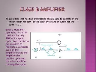
Push-Pull Nature of Class B • Push: The npn transistor will push the current to ground when the input is postive. • Pull: The pnp transistor will pull the current from the ground when the input is negative.
Crossover Distortion The Crossover Distortion is due to the dead band of input voltages from -.5V to .5V. This causes the Class B output stage to be a bad audio amplifier. For large input signals, the crossover distortion is limited, but at small input signals, it is most pronounced.
Graph of Crossover Distortion Fig. 9.7 Illustrating how the dead band in the class B transfer characteristic results in crossover distortion.
Power Efficiency Since each transistor is only conducting for one-half of the time, the power drawn from each source will be the same. Load Power: This efficiency will be at a max when Vop is at a max. Since Vop cannot exceed Vcc, the maximum efficiency will occur at pi/4. This will be approximately 78.5%, much greater than the 25% for Class A.
Small Signal Equivalent Fig.4.46 The common-collector or emitter-follower amplifier. (a) Circuit. (b) Equivalent circuit obtained by replacing the BJT with its T model. (c) The circuit in (b) redrawn to show that ro is in parallel with RL.(d) Circuit for determining Ro.