
Uploaded by
cleo
4 SLIDES
799 VUES
80LIKES
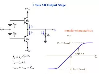
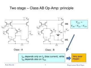
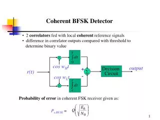
Class AB Output Stage
DESCRIPTION
Class AB Output Stage. transfer characteristic. Output Resistance. Biasing Class AB Circuit Using Diodes. If the junction area of the output devices, Q N and Q P , is n times that of the biasing devices D 1 and D 2 , a quiescent current I Q = n I BIAS flows in the output devices.
Download
1 / 4
Download Presentation

Télécharger la présentation
Class AB Output Stage
An Image/Link below is provided (as is) to download presentation
Download Policy: Content on the Website is provided to you AS IS for your information and personal use and may not be sold / licensed / shared on other websites without getting consent from its author.
Content is provided to you AS IS for your information and personal use only.
Download presentation by click this link.
While downloading, if for some reason you are not able to download a presentation, the publisher may have deleted the file from their server.
During download, if you can't get a presentation, the file might be deleted by the publisher.
E N D
Presentation Transcript
Class AB Output Stage transfer characteristic
Biasing Class AB Circuit Using Diodes If the junction area of the output devices, QN and QP, is n times that of the biasing devices D1 and D2, a quiescent current IQ = n IBIAS flows in the output devices.


More Related
Audio
Live Player