Download
1 / 18
360 likes | 961 Vues
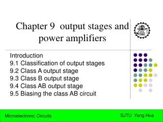
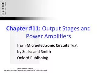
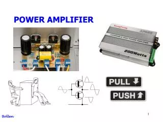
Chapter 14 Output stage and power amplifier. Introduction 14.1 Classification of output stage 14.2 Class A output stage 14.3 Class B output stage 14.4 Class AB output stage 14.5 Biasing the class AB circuit 14.6 Power BJT’s 14.7 Variation on the Class AB configuration

E N D
Introduction 14.1 Classification of output stage 14.2 Class A output stage 14.3 Class B output stage 14.4 Class AB output stage 14.5 Biasing the class AB circuit 14.6 Power BJT’s 14.7 Variation on the Class AB configuration 14.8 IC power amplifier 14.9 MOS power transistors
14.1 Classification of output stage conduction angle: 360o efficiency:25% to 50% conduction angle 180o efficiency :78.5% DC bias level DC bias level ‘0’ A class B class conduction angle 180o < θ<<360o conduction angle θ<< 180o AB class C class
14.2 A class output stage 14.2.1 Transfer characteristic Emitter follower (for large signal)
14.2.2 Signal waveform A class : maximum signal waveform
14.3 B class output stage 14.3.1 Circuit Operating npn pnp
14.3.2 Transfer Characteristic crossover distortion
14.3.5 Overcome Crossover distortion 14.3.6 Single power B-class
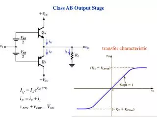
14.4 AB- class output stage 14.4.1 Circuit Operating
14.4.2 Output resistance 14.5 AB- class circuit bias 14.5.1 Using diode temperature compensation (prevent thermal runaway)
14.6 Power BJT 14.6.3 Power consumption & temperature 14.6.1 Junction temperature 14.6.2 Thermal resistance
14.6.4 BJT case & heat sink heat sink