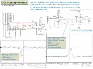
two-stage amplifier status
two-stage amplifier status. recent / final (hopefully) design uses load resistor and voltage gain stage for input; this is faster, lower noise, and more robustly stable 3.5 V supply voltage to minimize power and to limit output to safe input range of IRSX ASIC. G. Visser , Indiana Univ.

two-stage amplifier status
E N D
Presentation Transcript
two-stage amplifier status • recent / final (hopefully) design uses load resistor and voltage gain stage for input; this is faster, lower noise, and more robustly stable • 3.5 V supply voltage to minimize power and to limit output to safe input range of IRSX ASIC G. Visser, Indiana Univ. 0.5× −9× isignal 10× test buffer – to be replaced with IRSX typical output pulse (same conditions, different event) PMT pulse @ 3200 V 600 psrisetime 300 mV peak (to IRSX) typical PMT pulse @ 3200 V single photoelectron 200 psrisetime 8 mV peak (on 25 Ω load)
two-stage amplifier status 3200 V PMT gain ~ 3 × 10⁵ G. Visser, Indiana Univ. direct to scope (Zgain = 25 Ω) arbitrary scale – not counts! two-stage amp (Zgain = 3188 Ω) at 3200V, 89% of pulses are >50 mV reasonably flat response -3dB BW ~750 MHz input-referred noise ~1.33 nV/sqrt(Hz) 3200V 8 μV/div @ 1 MHz BW 150 MHz/div 3700V
new front board status • connects to boardstack via pogo pins (on boardstack, landing pads on front board) enables mating with misalignment tolerance • “radical” design of signal routing using thick multilayer board with blind holes decouples PMT and readout board pad locations (both sides have their firm constraints), and reduces routing length for improved high speed signal integrity signal trace routing in progress (90% complete) press-fit pin receptacle for PMT (shown on preamp test board)
below here is backup / for reference / for our detailed discussion as needed
iTOP two-stage preamp update G. Visser / IU November 11th 2013 • this is the “final” circuit configuration • except: • calibration signal path still t.b.d. • resistor values may change (dependent on pcb layout parasitics) isignal • 1st stage noninverting for lowest noise and more constant input impedance • gain = 10× • 2nd stage inverting for required output polarity • inverting amp can also be used to sum in calibration signal (without degrading risetime of PMT signal) • gain = −9× (or less...) • 3.5V supply limits output swing to protect the ASIC • test buffer – to be replaced with IRSX • DC coupled • signal current return through VREF plane, AC coupled to bottom of 2nd MCP • bury the signal lines in front and carrier board for shielding (from, e.g., digital crosstalk)
amplified single-photoelectron pulses @ -3200 V roughly 3×10⁵ gain (see later slide) risetime histogram (from scope) 100 mV/div 1.25 ns/div a typical pulse arbitrary scale – not counts! 578 psrisetime 300 mV peak Tek DPO7254C
raw single-photoelectron pulse @ -3200 V This is a somewhat larger than average pulse: Voltage on 25 Ω load (double-terminated cable) 2 mV/div 1.25 ns/div ≈200 psrisetime ≈500 ps width The noise and bandwidth limitations of this scope are significant here. The true pulse is likely rather faster and quieter.
pulse integral spectrum @ 3200V roughly 3×10⁵ gain (average charge) direct to scope (Zgain = 25 Ω) two-stage amp (Zgain = 3188 Ω) • Gate = 11 ns • Some double pulses and afterpulses are counted here • Zgain above (used for X axis scale) are design values, not calibrated
pulse peak amplitude spectrum counts (linear scale) 3200V 3700V at 3200V, 89% of pulses are >50 mV
pulse peak amplitude spectrum JT0298 PMT counts (linear scale)
slew rate limitation At the observed 600 ps small-signal risetime, this becomes an issue when pulse height >≈ 800 mV. There may be an extra “time walk” due to this for large pulses; needs consideration and/or avoidance. 3200V 3700V
noise (and gain flatness) 8 μV/div @ 1 MHz BW 150 MHz/div Note this is a linear scale (to better show gain/noise flatness). The peak at ~100 MHz is a local radio station. With −90× gain, the input referred noise is about 1.33 nV/sqrt(Hz).
front board (dummy version) everything seems to fit fine...