Download
1 / 28
370 likes | 893 Vues
Two Stage Amplifier Design. ENGI 242 ELEC 222. HYBRID MODEL PI. HYBRID MODEL PI PARAMETERS. Parasitic Resistances r b = r b’b = ohmic resistance – voltage drop in base region caused by transverse flow of majority carriers, 50 ≤ r b ≤ 500

E N D
Two Stage Amplifier Design ENGI 242 ELEC 222
HYBRID MODEL PI ENGI 242/ELEC 222
HYBRID MODEL PI PARAMETERS • Parasitic Resistances • rb = rb’b = ohmic resistance – voltage drop in base region caused by transverse flow of majority carriers, 50 ≤ rb ≤ 500 • rc = rce = collector emitter resistance – change in Ic due to change in Vc, 20 ≤ rc ≤ 500 • rex = emitter lead resistance – important if IC very large, 1 ≤ rex ≤ 3 ENGI 242/ELEC 222
HYBRID MODEL PI PARAMETERS • Parasitic Capacitances • Cje0 = Base-emitter junction (depletion layer) capacitance, 0.1pF ≤ Cje0 ≤ 1pF • C0 = Base-collector junction capacitance, 0.2pF ≤ C0 ≤ 1pF • Ccs0 = Collector-substrate capacitance, 1pF ≤ Ccs0 ≤ 3pF • Cje = 2Cje0 (typical) • 0 =.55V (typical) • F = Forward transit time of minority carriers, average of lifetime of holes and electrons, 0ps ≤ F ≤ 530ps ENGI 242/ELEC 222
HYBRID MODEL PI PARAMETERS • r = rb’e = dynamic emitter resistance – magnitude varies to give correct low frequency value of Vb’e for Ib • r = rb’c = collector base resistance – accounts for change in recombination component of Ib due to change in Vc which causes a change in base storage • c = Cb’e = dynamic emitter capacitance – due to Vb’e stored charge • c = Cb’c = collector base transistion capacitance (CTC) plus Diffusion capacitance (Cd) due to base width modulation • gmV = gmVb’e = Ic – equivalent current generator ENGI 242/ELEC 222
Hybrid Pi Relationships = gm r ENGI 242/ELEC 222
Hybrid Pi Relationships ENGI 242/ELEC 222
Design of a Two Stage Amplifier ENGI 242/ELEC 222
Two Stage Amplifier Design Specifications Design a two stage common emitter amplifier with partial emitter bypass for the following specifications: VCC = 20V VE = .1VCC RE1A = .25RE1 VC1 = .6VCC IC1 = 2mA RE2A = .4RE2 VC2 = .55VCC IC2 = 2.5mA R2 = .1RE1 R4 = .1RE2 RL = 10k fCL1 = 16Hz fCL2 = 13Hz fCL3 = 12Hz fCL4 = 67Hz fCL5 = 8Hz For both stages: = 140 CB = 150ps VA = 100V C 8pF fT = 150MHz rb = 19 ENGI 242/ELEC 222
Hybrid Pi Model ENGI 242/ELEC 222
Low Critical Frequencies • There is one low critical frequency for each coupling and bypass capacitor • We start by determining the (Thevenin) impedance seen by each capacitor • Then we construct a RC high pass filter (output across Z) • We may then calculate the critical frequency by letting |XC| = Z and solving for either fCL or C and fCL = fCL1 + fCL2 + fCL3 + fCL4 + fCL5 ENGI 242/ELEC 222
Hybrid Pi Model Input First Stage ENGI 242/ELEC 222
Hybrid Pi Model Output First Stage ENGI 242/ELEC 222
Hybrid Pi Model Input Second Stage ENGI 242/ELEC 222
Hybrid Pi Model Output Second Stage ENGI 242/ELEC 222
Hybrid Pi Model Emitter Bypass First Stage ENGI 242/ELEC 222
Hybrid Pi Model Emitter Bypass Second Stage ENGI 242/ELEC 222
fCL1 ENGI 242/ELEC 222
fCL2 Determine the Thevenin Impedance seen by C2 ENGI 242/ELEC 222
fCL3 Determine the Thevenin Impedance seen by C3 ENGI 242/ELEC 222
fCL4 Determine the Thevenin Impedance seen by CE1 ENGI 242/ELEC 222
fCL5 Determine the Thevenin Impedance seen by CE2 ENGI 242/ELEC 222
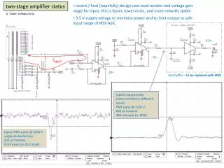
Schematic of Design ENGI 242/ELEC 222
Simulation Profile ENGI 242/ELEC 222
Probe Plot – Y Axis Settings ENGI 242/ELEC 222
Probe Plot – X Axis X Grid Settings ENGI 242/ELEC 222
Frequency Response ENGI 242/ELEC 222
Frequency Response ENGI 242/ELEC 222