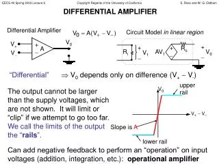
Practical Differential Amplifier Design
Practical Differential Amplifier Design. We’ve discussed Large signal behaviour Small signal voltage gain Today: Input impedance Output impedance Coupling & biasing D.C. effects Comparisons with the common-emitter amplifier. Input and Output Impedances.

Practical Differential Amplifier Design
E N D
Presentation Transcript
Practical Differential Amplifier Design We’ve discussed • Large signal behaviour • Small signal voltage gain Today: • Input impedance • Output impedance • Coupling & biasing • D.C. effects • Comparisons with the common-emitter amplifier
Input and Output Impedances An equivalent small signal circuit of a differential amplifier can be drawn as:
But, Input Impedance During the small signal analysis, it was shown that:
Applying Kirchoff’s current law: By Ohm’s law: Output Impedance NB. Same result as common emitter amplifier
Coupling and Biasing • Input and output coupling capacitors may be required to remove d.c. bias voltages • If input coupling capacitors are used, a d.c. bias current path to the transistors’ bases must be established • Extra base resistors accomplish this • These will appear in parallel with the input impedance
Constant Current Source • Current, I, should be constant regardless of varying VE • In practice, during small signal operation VE doesn’t vary by more than a fraction of a volt so a resistor is a good approximation (as in the lab experiment) • For a better approximation, a current mirror is often used
So, Exact equilibrium value of VBE is set by negative feedback and can be found from: Current Mirror VBE is unknown, but should be around 0.5 V VBE
But we know, Current Mirror (cont) VBE is identical for both transistors and So,
Non-Ideal D.C. Effects • If operation down to d.c. is required, the coupling components are omitted • This leads to some effects that are peculiar to d.c. operation: • Offset Voltage • Bias Current
Offset Voltage • With zero differential input, the collector currents and, therefore, the collector voltages should be identical • This assumes that: • The transistors are identical • The loads are also identical • In practice, loads will vary and the quiescent conditions will not be perfectly symmetrical • There will be an offset voltage between the actual output and the ideal assumption
Bias Current • In order to bring the transistors into the active region, a small d.c. base bias current is required • This d.c. current must be supplied by the signal source • This is a separate issue to the current drawn by the input impedance • Note that bias current and offset voltage effects are identical to those observed with op-amps
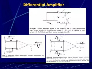
Noisy Channel Noisy received signals Difference Amp Output Transmitter Applications • Differential inputs and outputs • Useful when negative feedback is required in a multi-stage amplifier • Also useful for balanced signals
Comparisons with CE Amp • Common Emitter Features • One transistor required • Single input, single output • Maximum input amplitude for linear operation around 1 mV • High gain possible with high input impedance • Differential Features • At least two transistors required • Differential input, differential output • Maximum input amplitude for linear operation around 50 mV • Reduced gain possible with high input impedance
Multi-Stage Amplifiers • With both common-emitter amplifiers and differential amplifiers, a design compromise must be struck between: • Voltage gain • Input impedance • Output impedance • Simultaneously achieving specified requirements may not be possible using a single amplifier • Solution: cascade more than one amplifier in series • More on this next time…