Download
1 / 31
401 likes | 1.21k Vues
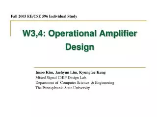
Fall 2005 EE/CSE 596 Individual Study. W3,4: Operational Amplifier Design. Insoo Kim, Jaehyun Lim, Kyungtae Kang Mixed Signal CHIP Design Lab. Department of Computer Science & Engineering The Pennsylvania State University. 2 Stage OP Amp Design. 2 Stage OP Amp. Frequency Compensation.

E N D
Fall 2005 EE/CSE 596 Individual Study W3,4: Operational Amplifier Design Insoo Kim, Jaehyun Lim, Kyungtae Kang Mixed Signal CHIP Design Lab. Department of Computer Science & Engineering The Pennsylvania State University
2 Stage OP Amp Frequency Compensation
[Reminder] Common Mode • Common Mode Gain • Common Mode Rejection Ratio • Common Mode Input Voltage Range VSS+VTN1+VDSAT5+VDSAT1 < VIC < VDD–|VDSAT3|–|VTP3|+| VTN1|
2 Stage OP Amp Design • Design Process • Model Parameter Extraction (1/6) • kn : 55.84 uA/V2 - kp : 23.51 uA/V2 • n : 0.025 - p : 0.055 • Vthn : 0.776 V - Vthp : 0.858 V • Assign Current from Power Consumption Spec. (2/6) • Power Consumption : 2 mW • Total Current : 0.4 mA @ 5V VDD • Input Pair : 0.2 mA • Second Stage : 0.2 mA
2 Stage OP Amp Design • Design Process • Determine minimum channel length (3/6) • Determine channel width (4/6) • Determine W1,2 from voltage gain spec. • Determine W5 & Bias Voltagefrom power consumption & CM min. • Determine W3,4 from CM max. • Determine Bias Level of Current Source Tr. (5/6) • Considering CM min value and the transistor size • Check other specifications (6/6) • Repeat step 4 to 6
A Calculation Example Calculated Gain= 3000 (70dB)
Simulation Results This OP Amp is unstable! Gain: 59dB BW: 1.15 GHz
Vin + - Vout Before Frequency Compensation • A unit gain buffer characteristic without frequency compensation
Positive Zero & Pole-Zero Cancellation • Feed Forward
Positive Zero & Pole-Zero Cancellation • Pole-Zero Cancellation
An Example of Frequency Compensation Poles moved!
Vin + - Vout After Frequency Compensation • A unit gain buffer characteristic with frequency compensation Frequency compensated OP Amp Frequency Compensation must be considered in designing OP Amps
Folded Cascode Op Amp Basic Folded Cascode Design of Single Ended Folded Cascode
Cascode Stage • Small Signal Analysis • Rout
Folded Cascode Stage • Schematic • Advantages • Wider Operating Range than telescopic cascode stage • Easy to set Common Mode Voltage • Disadvantages • Limited Output swing • Large Voltage Headroom • Large Power Consumption
Single Ended Folded Cascode Op Amp • Circuit Configuration
(cont’d) Single Ended Folded Cascode Op Amp • Design Process (1/3) • Model Parameter Extraction • kn : 55.84 uA/V2 - kp : 23.51 uA/V2 • n : 0.025 - p : 0.055 • Vthn : 0.776 V - Vthp : 0.858 V • Assign Current from Power Consumption Spec. • Total Current : 0.375 mA • Input pair : 0.125 mA • Current mirror : 0.25 mA
(cont’d) Single Ended Folded Cascode Op Amp • Design Process (2/3) • Determine W3 from CM_min, CM_max Spec. • CM_min • CM_max • Determine W4~W7 and Bias2 from Vout_max Spec. • Vout_max : Determine VB2 • Assign Vdsat of M4,5 and M6,7 from Vout_max Spec • Eg) Vout_max=4V Vdsat of M4,5= 0.6V, Vdsat of M6,7 = 0.4V • Calculate W4~7 to satisfy Vdsat & Ids of M4~7 • Determine W8~W11 from Vout_min Spec. • Assign Vdsat of M8~M11 from Vout_min Spec. • Eg) Vout_min=0.8V Vdsat of M8~11 = 0.4V • Calculate W8~11 to satisfy Vdsat and Ids of M8~11
(cont’d) Single Ended Folded Cascode Op Amp • Design Process (3/3) • Determine W1,2 from Gain Spec. • Calculate Rout_tot • Calculate Required Gm value to satisfy Gain Spec. • Gain = Gm*Rout • Calculate W1,2 from Gm • Check other Spec. and Repeat the design process to optimize transistors size • Slew Rate • CM_min Check required • CMRR, PSRR • Check and Modify Bias Voltage to optimize transistor size.
(cont’d) Single Ended Folded Cascode Op Amp • Frequency Analysis
3.54V 53.1 53.1 89.7 3.14V 89.7 68.1 68.1 39.75 39.75 80.25 39.75 39.75 1.0V (cont’d) Single Ended Folded Cascode Op Amp • Design Example Calculated Gain= 3000 (70dB)
(cont’d) Single Ended Folded Cascode Op Amp • Simulation Result Gain: 68dB BW: 170MHz Loading: 2pF
References • Joongho Choi, “CMOS analog IC Design,” IDEC Lecture Note, Mar. 1999. • B. Razavi, “Design of Analog CMOS Integrated Circuits,” McGraw-Hill, 2001. • Hongjun Park, “CMOS Analog Integrated Circuits Design,” Sigma Press, 1999.