Chapter 15 Differential Amplifiers and Operational Amplifier Design
1.67k likes | 3.71k Vues
Chapter 15 Differential Amplifiers and Operational Amplifier Design. Microelectronic Circuit Design Richard C. Jaeger Travis N. Blalock. Chapter Goals. Explore dc and ac properties of differential amplifiers. Understand basic three-stage op amp.

Chapter 15 Differential Amplifiers and Operational Amplifier Design
E N D
Presentation Transcript
Chapter 15Differential Amplifiers and Operational Amplifier Design Microelectronic Circuit Design Richard C. Jaeger Travis N. Blalock Microelectronic Circuit Design, 3E McGraw-Hill
Chapter Goals • Explore dc and ac properties of differential amplifiers. • Understand basic three-stage op amp. • Explore design of class-A, class-B, class-AB output stages. • Discuss characteristics and design of electronic current sources. • Understand bipolar and MOS current mirror operation and mirror ratio errors. • Explore high output resistance current sources. • Design current sources for both discrete and integrated applications. • Study reference current circuits such as VBE-based reference, bandgap reference and Widlar current source. • Use current mirrors as active loads in differential amplifiers to increase voltage gain of single-stage amplifiers. • Study effects of device mismatch on amplifier performance. • Analyze design of classic mA741 op amp. • Increase understanding of SPICE simulation techniques. Microelectronic Circuit Design, 3E McGraw-Hill
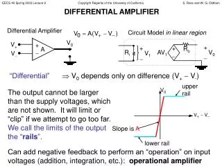
Differential Amplifiers • Each circuit has two inputs. • Difference of the two inputs is the differential input. • Differential-mode output voltage is the voltage difference between collectors, drains of the two transistors. • Ground referenced outputs can also be taken from collector/drain. • Ideal differential amplifier uses perfectly matched transistors. Microelectronic Circuit Design, 3E McGraw-Hill
Bipolar Differential Amplifiers: DC Analysis Terminal currents are also equal. Both inputs are set to zero, emitters are connected together. If transistors are matched, Microelectronic Circuit Design, 3E McGraw-Hill
Small-Signal Transfer Characteristic The current switch is a digital application of the differential amplifier. Large-signal transfer characteristic of differential amplifier is given by: Even-order distortion terms are eliminated.This increases signal-handling capability of differential pair. For small-signal operation, linear term must be dominant. Hence, we set the third-order term to be one-tenth the linear term. Microelectronic Circuit Design, 3E McGraw-Hill
Bipolar Differential Amplifiers: DC Analysis (Example) • Problem:Find Q-points of transistors in the differential amplifier. • Given data:VCC=VEE=15 V, REE=RC=75kW, bF =100 • Analysis: Due to symmetry, both transistors are biased at Q-point (94.4 mA, 8.62V) Microelectronic Circuit Design, 3E McGraw-Hill
Bipolar Differential Amplifiers: AC Analysis Add = differential-mode gain Acd = common-mode to differential-mode conversion gain Acc = common-mode gain Adc = differential mode to common-mode conversion gain For ideal symmetrical amplifier, Acd = Adc = 0. Purely differential-mode input gives purely differential-mode output and vice versa. Circuit analysis is done by superposition of differential-mode and common-mode signal portions. Microelectronic Circuit Design, 3E McGraw-Hill
Bipolar Differential Amplifiers: Differential-mode Gain and Input Resistance Emitter node in differential amplifier represents virtual ground for differential-mode input signals. Output signal voltages are: Microelectronic Circuit Design, 3E McGraw-Hill
Bipolar Differential Amplifiers: Differential-mode Gain and Input Resistance (cont.) Differential-mode gain for balanced output, is: If either vc1 or vc2 is used alone as output, output is said to be single-ended. Differential-mode input resistance is small-signal resistance presented to differential-mode input voltage between the two transistor bases. If vid =0, . For single-ended outputs, Microelectronic Circuit Design, 3E McGraw-Hill
Bipolar Differential Amplifiers: Common-mode Gain and Input Resistance Both arms of differential amplifier are symmetrical. So terminal currents and collector voltages are equal. Characteristics of differential pair with common-mode input are similar to those of a C-E (or C-S) amplifier with large emitter (or source) resistor. Output voltages are: Microelectronic Circuit Design, 3E McGraw-Hill
Bipolar Differential Amplifiers: Common-mode Gain and Input Resistance (cont.) Common-mode gain is given by: For symmetrical power supplies, common-mode gain =0.5. Thus, common-mode output voltage and Acc is 0 if REE is infinite. This result is obtained since output resistances of transistors are neglected. A more accurate expression is: Therefore, common-mode conversion gain is found to be 0. Microelectronic Circuit Design, 3E McGraw-Hill
Common-Mode Rejection ratio (CMRR) • Represents ability of amplifier to amplify desired differential-mode input signal and reject undesired common-mode input signal. • For differential output, common-mode gain of balanced amplifier is zero, CMRR is infinite. For single-ended output, • For infinite REE , CMRR is limited by bomf . If term containing REE is dominant Thus for differential pair biased by resistor REE , CMRR is limited by available negative power supply. • Due to mismatches, , gives fractional mismatch between small-signal device parameters in the two arms of differential pair. Hence gmREE product is maximized. Microelectronic Circuit Design, 3E McGraw-Hill
Analysis of Differential Amplifiers Using Half-Circuits • Half-circuits are constructed by first drawing the differential amplifier in a fully symmetrical form- power supplies are split into two equal halves in parallel, emitter resistor is separated into two equal resistors in parallel. • None of the currents or voltages in the circuit are changed. • For differential mode signals, points on the line of symmetry are virtual grounds connected to ground for ac analysis • For common-mode signals, points on line of symmetry are replaced by open circuits. Microelectronic Circuit Design, 3E McGraw-Hill
Bipolar Differential-mode Half-circuits Direct analysis of the half-circuits yield: Applying rules for drawing half-circuits, the two power supply lines and emitter become ac grounds. The half-circuit represents a C-E amplifier stage. Microelectronic Circuit Design, 3E McGraw-Hill
Bipolar Common-mode Half-circuits • All points on line of symmetry become open circuits. • DC circuit with VIC set to zero is used to find amplifier’s Q-point. • Last circuit is used for for common-mode signal analysis and represents the C-E amplifier with emitter resistor 2REE. Microelectronic Circuit Design, 3E McGraw-Hill
Bipolar Common-mode Input Voltage Range For symmetrical power supplies, VEE >> VBE, and RC = REE, Microelectronic Circuit Design, 3E McGraw-Hill
Biasing with Electronic Current Sources • Differential amplifiers are biased using electronic current sources to stabilize the operating point and increase effective value of REE to improve CMRR • Electronic current source has a Q-point current of ISS and an output resistance of RSS as shown. • DC model of the electronic current source is a dc current source, ISS while ac model is a resistance RSS. SPICE model includes both ac and dc models. Microelectronic Circuit Design, 3E McGraw-Hill
MOSFET Differential Amplifiers: DC Analysis and Op amps with MOSFET inputs have a high input resistance and much higher slew rate that those with bipolar input stages. Using half-circuit analysis method, we see that IS = ISS /2. Microelectronic Circuit Design, 3E McGraw-Hill
Small-Signal Transfer Characteristic MOS differential amplifier gives improved linear input signal range and distortion characteristics over that of a single transistor. Second-order distortion product is eliminated and distortion is greatly reduced. However some distortion prevails as MOSFETs are nor perfect square law devices and some distortion arises through voltage dependence of output impedances of the transistors. For symmetrical differential amplifier with purely differential-mode input Microelectronic Circuit Design, 3E McGraw-Hill
MOSFET Differential Amplifiers: DC Analysis (Example) • Problem:Find Q-points of transistors in the differential amplifier. • Given data:VDD=VSS=12 V, ISS =200 mA, RSS = 500 kW, RD = 62 kW,l = 0.0133 V-1, Kn = 5 mA/ V2, VTN =1V • Analysis: To maintain pinch-off operation of M1 for nonzero VIC , Microelectronic Circuit Design, 3E McGraw-Hill
MOSFET Differential Amplifiers: Differential-mode Input Signals Source node in differential amplifier represents virtual ground Differential-mode gain for balanced output is Gain for single-ended output is Microelectronic Circuit Design, 3E McGraw-Hill
MOSFET Differential Amplifiers: Common-mode Input Signals Electronic current source is modeled by twice its small-signal output resistance representing output resistance of the current source. Common-mode half-circuit is similar to inverting amplifier with 2RSS as source resistor. Thus, common-mode conversion gain= 0 Due to infinite current gain of FET, ro can be neglected. Microelectronic Circuit Design, 3E McGraw-Hill
Common-Mode Rejection ratio (CMRR) • For purely common-mode input signal, output of balanced MOS amplifier is zero, CMRR is infinite. For single-ended output, • RSS (which is much > REE and thus provides more Q-point stability) should be maximized. • To compare MOS amplifier directly to BJT amplifier, assume that MOS amplifier is biased by • From given data in example, MOS amplifier’s CMRR=54 or 35 dB (almost 10 dB worse than BJT amplifier).To increase CMRR in BJT and FET amplifiers, current sources with higher RSS or REE are used. Microelectronic Circuit Design, 3E McGraw-Hill
Two-port model for Differential Amplifiers Two-port model simplifies circuit analysis of differential amplifiers. Expressions for FET are obtained by substituting RSS for REE. Microelectronic Circuit Design, 3E McGraw-Hill
Differential Amplifier Design (Example) • Problem:Find Q-points of transistors in the differential amplifier. • Given data:Adm=40 dB, Rid >250 kW,single-ended CMRR> 80 dB, VICat least ±5V, MOSFETs with: l = 0.0133 V-1, Kn’ = 50 mA/ V2, VTN =1V, • BJTs with : bF =100, VA =75V, IS =0.5 fA • Assumptions: Active-region operation, symmetrical power supplies, bo = bF, vid maximum of ±30 mV. • Analysis: • Adm=40 dB =100. To achieve this gain with resistively loaded amplifier, we use BJT. For Adm = gm RC =40 IC RC , required gain can be obtained with voltage drop of 2.5 V across RC. • For bipolar differential amplifier, Rid =2rp, so, rp =125 kW. Microelectronic Circuit Design, 3E McGraw-Hill
Differential Amplifier Design (Example cont.) Choose IC = 15 mA to provide safety margin. So RC =2.5 V/15 mA =167 kW. Choose RC = 180 kW as the nearest value with 5% tolerance and also to compensate for neglecting ro in the analysis. VICof 5V requires collector voltage to be at least 5 V at all times. We also know that vid can be a maximum of ±30 mV for linearity. So ac component of differential output will not be greater than 100(0.03 V)=3V, half of which appears at each collector. Thus dc signal across RC won’t exceed 4 V( 2.5 V dc + 1.5 V ac) and positive power supply must fulfill Choose VCC=10 V to dive desired margin of 1 V, For symmetrical supplies, VEE = -10 V. Single-ended CMRR of 80 dB needs Choose current source with IEE =30 mA and REE > 20 MW Microelectronic Circuit Design, 3E McGraw-Hill
Two-stage Prototype of an Op Amp • For higher gain, pnp C-E amplifier is connected at output of the input stage differential amplifier. • Virtual ground at emitter node allows input stage to achieve full inverting amplifier gain without needing emitter bypass capacitor. • PNP transistor permits direct coupling between stages, allows emitter of pnp to be connected to ac ground and provides required voltage level shift to bring output back to zero. • Bypass and coupling capacitors are thus eliminated. Differential amplifier provides desired differential input,CMRR and ground referenced output as the input stage of op amp. Microelectronic Circuit Design, 3E McGraw-Hill
Two-stage Op Amp: DC Analysis This circuit requires a resistance in series with emitter of Q3 to stabilize Q-point (as collector current of Q3 is exponentially dependent on base-emitter voltage), at the expense of voltage gain loss. From dc equivalent circuit, IE1= IE2 = I1 /2. If base current of Q3 is neglected and C-B current gains are one, As both inputs are zero, output also=0 IS3 is saturation current. For zero offset voltage Microelectronic Circuit Design, 3E McGraw-Hill
Two-stage Op Amp: AC Analysis (Differential Mode) Half-circuit can be constructed from ac equivalent circuit in spite of asymmetry, as voltage variations at collector of Q2 don’t substantially alter transistor current in forward-active operation region. From small-signal circuit model, Microelectronic Circuit Design, 3E McGraw-Hill
Two-stage Op Amp: AC Analysis (Differential Mode cont.) This can be rewritten as Base current of Q3 is neglected so, IC2RC=VBE3=0.7 V, IC3R=VEE, Upper limit onIC2 and I1 is set by maximum dc bias current at input, lower limit on IC3 is set by minimum current to drive total load impedance at output. Microelectronic Circuit Design, 3E McGraw-Hill
Two-stage Op Amp: AC Analysis (Common Mode) From ac equivalent circuit for common-mode inputs, For differential-mode inputs, collector current was Thus, From ac equivalent circuit, we observe that circuitry beyond collector of Q2 is same as that in differential mode half-circuit. The difference in collector currents causes difference in output voltage. Microelectronic Circuit Design, 3E McGraw-Hill
Improving Op Amp Voltage Gain Overall amplifier gain decreases rapidly as the quiescent current of second stage decreases. Voltage gain can improve if resistor in second stage is replaced by current source with R2 >> ro3, if R2 is neglected, This expression can be reduced to Because of the high output resistance the amplifier resembles a transconductance amplifier more than a true low output resistance voltage amplifier. Microelectronic Circuit Design, 3E McGraw-Hill
Reducing Output Resistance From ac equivalent circuit, A C-C stage is added to the prototype to maintain voltage gain but reduce output resistance. Microelectronic Circuit Design, 3E McGraw-Hill
Three-Stage Bipolar Op Amp Analysis • Problem: Find differential-mode gain, CMRR, input and output resistances. • Given data:VCC=VEE=15 V, bo1 = bo2 = bo3 = bo4 =100, VA3 =75V, I1 = 100 mA, I2 = 500 mA, I3 = 5 mA, R1 = 750 kW , RL = 2 kW, R2 and R3 are infinite. • Analysis: Voltage at node 3 is one base-emitter voltage drop above zero. VEC3=15-0.7=14.3 V. Microelectronic Circuit Design, 3E McGraw-Hill
Three-Stage Bipolar Op Amp Analysis (cont.) Overall gain is lower because of lower gain of first stage (since rp3 << RC) and lower gain than expected for second stage (as reflected loading of RL is of same order as ro3). Microelectronic Circuit Design, 3E McGraw-Hill
CMOS Op Amp Prototype: Circuit • Differential amplifier (M1 and M2) followed by C-S stage M3 and source follower M4. • Current sources are used to bias differential input and source follower stages and as load for M3. Microelectronic Circuit Design, 3E McGraw-Hill
CMOS Op Amp Prototype: AC Analysis Design freedom is higher than in bipolar case due to Q-point dependence of mf. Operating currents should be reduced and M3 should have small l to achieve higher gain.Input bias current doesn’t restrict ID1 as IG =0. Since source follower has unity gain, Microelectronic Circuit Design, 3E McGraw-Hill
BiCMOS Amplifiers • Integrated circuit processes with both BJT and MOS transistors or bipolar transistors and JFETs are called BiCMOS and BiFET technologies respectively. • Input PMOS transistors give high input resistance, can be biased at relatively high input currents, which can improve slew rate. • Second gain stage uses BJT with superior amplification factor than FET. • RE increases voltage across RD2 and hence the voltage gain of first stage without reducing amplification factor of Q1. • Follower stage uses another FET to maximize second-stage gain while maintaining reasonable output resistance. Microelectronic Circuit Design, 3E McGraw-Hill
Op Amp Output Stages • Output stage is designed to provide low output resistance and relatively high current drive capability. • Followers: Class-A amplifiers- transistors conduct during full 3600 of signal waveform, conduction angle =3600. • Push-pull: Class-B- each of the two transistors conducts during 1800of signal wavefrom, conduction angle =1800. • Class-AB: Characteristics of Class-A and Class-B are combined, most commonly used as output stage in op amps. Microelectronic Circuit Design, 3E McGraw-Hill
Source-Follower: Class-A Output Stage For a source-follower,difference between input and output voltages is fixed and voltage transfer characteristic is as shown. If load resistor is connected to output, total source current: vMIN = -ISS RL and iS=0, M1cuts off when vI = -ISS RL + VTN. Microelectronic Circuit Design, 3E McGraw-Hill
Source-Follower: Class-A Output Stage If output signal is given by: Efficiency of amplifier is given by: Low efficiency is due to current ISS that constantly flows between the two supplies. Microelectronic Circuit Design, 3E McGraw-Hill
Class-B Push-Pull Output Stage Improve efficiency by operating transistors at zero Q-point current eliminating quiescent power dissipation. NMOS transistor is a source-follower for positive input signals and NMOS transistor is a source-follower for negative input signals. Since neither transistor conducts when, output waveform suffers from a dead-zone or crossover distortion. Microelectronic Circuit Design, 3E McGraw-Hill
Class-AB Amplifiers The required bias voltage can be developed as shown.We assume that bias voltage splits equally between gate-source(or base-drain) terminals. Currents are given by Benefits of Class-B amplifier can be maintained without dead zone by biasing transistors into conduction but at a low quiescent current level (<< peak ac current delivered to load). For each transistor, 1800< conduction angle <3600. Microelectronic Circuit Design, 3E McGraw-Hill
Class-AB Output Stages for Op Amps Microelectronic Circuit Design, 3E McGraw-Hill
Short-Circuit Protection High current, high power dissipation or direct destruction of base-emitter junction can destroy the BJT if output of a follower circuit is accidentally shorted to ground. Q2 is added to protect the emitter follower. Normally, voltage across R is <0.7 V, Q2 is cutoff. Q2 turns on to shunt extra current away from base of Q1. IE1 is limited to For complementary output stage, similar current-limiting circuitry is used. In MOSFET complementary output stages, output current is limited to Microelectronic Circuit Design, 3E McGraw-Hill
Transformer Coupling: Follower Transformer provides impedance transformation by n2 . From ac equivalent circuit,transistor must drive Transformer restricts operation to frequencies >dc. Transformer coupling is used in amplifiers to achieve high voltage gain and efficiency while delivering power to low impedance loads. Coupling capacitor blocks dc path through primary of transformer. Microelectronic Circuit Design, 3E McGraw-Hill
Transformer Coupling: Inverting Amplifier and Class-B Output Stage Inductance permits signal voltage to swing symmetrically above and below VDD. As both quiescent operating currents = 0, emitters can be directly connected to transformer primary. At dc, transformer is a short circuit, quiescent operating current is supplied through transformer primary. At signal frequency load n2RL is presented to transistor. Microelectronic Circuit Design, 3E McGraw-Hill
Electronic Current Sources: Introduction • Current through ideal current source is independent of voltage across its terminals and the output resistance is infinite. • In electronic current sources, current depends on voltage across the terminals and they have a finite output resistance. • Single-transistor current sources operate in only one quadrant of i-v space but realize very high output resistances. Microelectronic Circuit Design, 3E McGraw-Hill
Current Sources: Figure of Merit is used as a figure of merit for comparing different current sources. For a given Q-point current, VCS represents the equivalent voltage that will be needed across a resistor to achieve same output resistance as given current source. For resistor: For BJT: For MOSFET: Microelectronic Circuit Design, 3E McGraw-Hill
Higher Output Resistance Sources For MOSFET: Output resistance of the current source can be increased by placing a resistor in series with the emitter or source of the transistor. For BJT: Microelectronic Circuit Design, 3E McGraw-Hill