4446 Design of Microprocessor-Based Systems
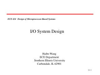
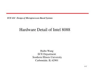
4446 Design of Microprocessor-Based Systems. Hardware Detail of Intel 8088. Dr. Esam Al_Qaralleh CE Department Princess Sumaya University for Technology. GND. VCC. 1. 40. A14. A15. 2. 39. A13. A16 / S3. 3. 38. A12. A17 / S4. 4. 37. A11. A18 / S5. 5. 36. A10. A19 / S6.

4446 Design of Microprocessor-Based Systems
E N D
Presentation Transcript
4446 Design of Microprocessor-Based Systems Hardware Detail of Intel 8088 Dr. Esam Al_Qaralleh CE Department Princess Sumaya University for Technology
GND VCC 1 40 A14 A15 2 39 A13 A16 / S3 3 38 A12 A17 / S4 4 37 A11 A18 / S5 5 36 A10 A19 / S6 6 35 A9 SS0 (High) 7 34 A8 MN / MX 8 33 AD7 RD 9 32 AD6 HOLD (RQ / GT0) 10 31 AD5 HLDA (RQ / GT1) 11 30 AD4 WR (LOCK) 12 29 AD3 IO / M (S2) 13 28 AD2 DT / R (S1) 14 27 AD1 DEN (S0) 15 26 AD0 ALE (QS0) 16 25 NMI INTA (QS1) 17 24 INTR TEST 18 23 CLK READY 19 22 GND RESET 20 21 8088 Pin Configuration
10.3 CPU pin descriptions Minmode operation signals (MN/MX=1) Time-multiplexed Address Bus /Status signals (outputs) 0V=“0”, reference for all voltages GND A14 A13 A12 A11 A10 A9 A8 AD7 AD6 AD5 AD4 AD3 AD2 AD1 AD0 NMI INTR CLK GND 1 40 8088 20 21 Vcc A15 A16/S3 A17/S4 A18/S5 A19/S6 ___ SS0 (HIGH) ___ MN/MX ___ RD ___ ____ HOLD (RQ/GT0) ___ ____ HLDA (RQ/GT1) ___ ______ WR(LOCK) __ __ IO/M(S2) __ __ DT/R(S1) ____ __ DEN(S0) ALE (QS0) _____ INTA (QS1) _____ TEST READY RESET 5V±10% Maxmode operation signals (MN/MX=0) Address Bus (outputs) Control Bus (in,out) Operation Mode, (input): 1 = minmode (8088 generates all the needed control signals for a small system), 0 = maxmode (8288 Bus Controller expands the status signals to generate more control signals) Time-multiplexed Address (outputs)/Data Bus (bidirectional) Status signals (outputs) Hardware interrupt requests (inputs) 2...5MHz, 1/3 duty cycle (input) Interrupt acknowledge (output)
8088 Pin Description Pin Name Pin Number Description Direction GND: 1 & 20 Both need to be connected to ground VCC: 21 VCC = 5V CLK: 19 Input 33% duty cycle 2/3*T 1/3*T MN/MX: 33 Input High Minimum mode Low Maximum mode RESET: 21 Input Reset 8088 • Duration of logic high must be greater than 4*T • After reset, 8088 fetches instructions starting from memory address FFFF0H
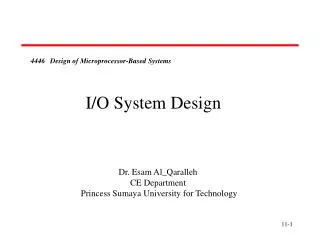
8088 READY Selected memoryor I/O device READY Data bus wait for memoryor I/O ready Start data transfer 8088 Pin Description Pin Name Pin Number Description Direction READY 22 Input Informs the processor that the selected memory or I/O device is ready for a data transfer
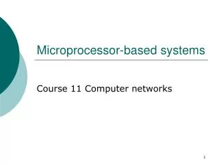
HOLD 8088 Device 2 HLDA Bus Memory 8088 Pin Description Pin Name Pin Number Description Direction HOLD 31 Input The execution of the processor is suspended as long as HOLD is high HLDA 30 Output Acknowledges that the processor is suspended • Procedure for Device 2 to use bus • Drive the HOLD signal of 8088 high • Wait for the HLDA signal of 8088 becoming high • Now, Device2 can send data to bus
INTR INTR 8088 INTA External device INTA Data Bus Int. type Data bus 8088 Pin Description Pin Name Pin Number Description Direction NMI 17 Input Causes a non-maskable type-2 interrupt INTR 18 Input Indicates a maskable interrupt request INTA 24 Output Indicates that the processor has received anINTR request and is beginning interruptprocessing • NMI (non-maskable interrupt): a rising edge on NMI causes a type-2 interrupt • INTR: logic high on INTR poses an interrupt request. However, this request can be masked by IF (Interrupt enable Flag). The type of interrupt caused by INTR is read from data bus • INTA: control when the interrupt type should be loaded onto the data bus
D Q G 8088 Pin Description Pin Name Pin Number Description Direction ALE 25 Output Indicates the current data on 8088 address/data bus are address A[19:8] Buffer A[19:8] ALE 8088 A[7:0] AD[7:0] D latches D[7:0]
8088 Pin Description Pin Name Pin Number Description Direction DEN 26 Output Disconnects data bus connection DT / R 27 Output Indicates the direction of data transfer DEN DT/R 1 X Disconnected 0 0 To 8088 0 1 From 8088 DEN 8088 DT/R D[7:0] Data bus DEN DT/ R AD[7:0]
8088 Pin Description Pin Name Pin Number Description Direction WR 29 Output Indicates that the processor is writing to memory or I/O devices RD 32 Output Indicates that the processor is reading from memory or I/O devices IO/ M 28 Output Indicates that the processor is accessing whethermemory (IO/M=0) or I/O devices (IO/M=1) WE WR or RD WR OE I/O RD Addr. Dec. CS Addr. Dec. Memory IO/M IO/M 8088
8088 Pin Description Pin Name Pin Number Description Direction AD[7:0] 9-16 I/O Address / Data bus A[19:8] 2-8, 35-39 Input Address bus SS0 34 Output Status Output TEST 23 Input It is examined by processor testing instructions LOCK 29 Input Lock output is used to lock peripherals off the system. Activated by using the LOCK: prefix on any instruction. QS1 and QS024, 25 Input The queue status bits show status of internal instruction queue. Provided for access by the numeric coprocessor (8087).
10.3 CPU pin descriptions MEMRD RD MEMWR WR IORD Decoding 8088 memory and I/O read/write signals IOWR IO/M 8088 Status Signals 8088 Signal Summary Comparison of NMI and INTR
8284 Clock Generator 8284 8088 • Basic functions: • Clock generation. • RESET synchronization. • READY synchronization. • Peripheral clock signal. RDY1 Ready1 Ready2 RDY2 Ready Ready X1 510 CLK CLK X2 510 +5V RESET RESET RES 100K • Generates 33% duty cycle clock signal • Generates RESET signal • Synchronizes ready signals from memory and I/O devices 10uF
10.4 The 8284 Clock Generator 5V READY1 CLK 8088 READY RESET RDY1 RDY2 EFI CLK F/C CSYNC AEN1 AEN2 8284 ASYNC X1READY X2RESRESET READY2 0 = crystal oscillator 1 = TTL clock on EFI, synchronized on CSYNC 4K7 qualifiers for READY1,-2 5V 2X510 1 = one WAIT state forced by READY CLK 10MHz 100K 0 = forces the P to froze the current bus cycle inserting WAIT STATES (all signals keep their values), allowing slower devices time to properly answer. 10F 5V 1N4148 1/3 fosc 1/3 duty cycle RES [V] t X1,2 [V] RESET 1L 0L t t
8288 Bus Controller • Separate signals are used for I/O ( IORC and IOWC ) and memory ( MRDC and MWTC ). • Also provided are advanced memory ( AIOWC ) and I/O ( AIOWC ) write strobes plus INTA .
10.5 The 8288 Bus Controller 74LS244 G1 G2 CPU Address Bus (A16-A19, if needed, should be latched the same way like AD0-AD7) Identify the Memory Byte (one of 220 (216 in example)) OR the I/O port (one of 216) to be read OR write in the current bus cycle A8-A15 AD0-AD7 8088 S0 S1 S2 8282 STB OE D Q LE Advanced Write Commands, providing additional access time for the selected circuit Data to be transferred in the current bus cycle 8286 OE T Max one active at a time, identifying Memory vs. I/O and Read vs. Write CPU Data Bus Data Transmit/Receive DENDT/RMRDC ALEMWTC S0IORC S1 8288 IOWC S2INTA AMWC AIOWC IOB AEN CEN Address Latch Enable Status Signals (codify the bus cycle type) 5V Command Enable Control Bus Address Enable I/O Bus only CLK Data Enable Memory ReaD Command Memory WriTe Command Input/Output Read Command Input/Output Write Command INTerrupt Acknowledge Advanced Memory Write Command Advanced Input/Output Write Command
System Timing Diagrams • T-State: • One clock period is referred to as a T-State T-State • An operation takes an integer number of T-States • CPU Bus Cycle: • A bus cycle consists of 4 or more T-States T1 T2 T3 T4
Memory Read Timing Diagrams • Dump address on address bus. • Issue a read ( RD ) and set M/ IO to 1. • Wait for memory access cycle.
Memory Read Timing Diagrams T3 T4 T2 T1 CLK A[15:8] ALE Buffer A[15:0] 8088 A[19:16] A[19:16] S3-S6 AD[7:0] A[15:8] A[15:8] D latch Memory AD[7:0] A[7:0] D[7:0] IO/M D[7:0] Trans -ceiver DT/R DT/R DEN DEN IO/M RD WR RD WR
Memory Write Timing Diagrams • Dump address on address bus. • Dump data on data bus. • Issue a write ( WR ) and set M/ IO to 1.
Memory Write Timing Diagrams T3 T4 T2 T1 CLK A[15:8] ALE Buffer A[15:0] 8088 A[19:16] A[19:16] S3-S6 AD[7:0] A[15:8] A[15:8] D latch Memory AD[7:0] A[7:0] D[7:0] IO/M D[7:0] Trans -ceiver DT/R DT/R DEN DEN IO/M RD WR RD WR
Bus Timing During T 1 : • The address is placed on the Address/Data bus. • Control signals M/ IO , ALE and DT/ R specify memory or I/O, latch the address onto the address bus and set the direction of data transfer on data bus. During T 2 : • 8086 issues the RD or WR signal, DEN , and, for a write, the data. • DEN enables the memory or I/O device to receive the data for writes and the 8086 to receive the data for reads. During T 3 : • This cycle is provided to allow memory to access data. • READY is sampled at the end of T 2 . • If low, T 3 becomes a wait state. • Otherwise, the data bus is sampled at the end of T 3 . During T 4 : • All bus signals are deactivated, in preparation for next bus cycle. • Data is sampled for reads, writes occur for writes.
Setup & Hold Time • Setup time – The time before the rising edge of the clock, while the data must be valid and constant • Hold time – The time after the rising edge of the clock during which the data must remain valid and constant
Bus Timing Timing: • Each BUS CYCLE on the 8086 equals four system clocking periods (T states). • The clock rate is 5MHz , therefore one Bus Cycle is 800ns. • The transfer rate is 1.25MHz. Memory specs (memory access time) must match constraints of system timing. For example, bus timing for a read operation shows almost 600nsare needed to read data. • However, memory must access faster due to setup times, e.g. Address setup and data setup. • This subtracts off about 150ns. • Therefore, memory must access in at least 450nsminus another 30-40nsguard band for buffers and decoders. • 420nsDRAM required for the 8086.
10.6 System Time Diagrams - CPU Bus Cycle T1 T2 T3 TW T4 CLK ALE Address latches store the actual values Memory Cycle (I/O cycle is similar but IO/M = 1) IO/M A16- A19 A16-A19 S3- S6 A8- A15 A8- A15 READY the P samples READY (if 0 a WAIT state follows) The slow device drives READY= 0 Read Cycle (instruction fetch and memory operand read) RD P reads Data Bus AD0- AD7 A0- A7 D0- D7 (Data in) Tri-state DT/R Direction “READ” for the Data Buffer DEN Enables Data Buffer Memory reads Data Bus WR Write Cycle (memory operand write) AD0- AD7 A0- A7 D0- D7 (Data out) DT/R Direction “READ” for the Data Buffer DEN Enables Data Buffer
INTR 8088 External device INTA Data bus Interrupt Acknowledge Timing Diagrams T3 T4 T2 T1 CLK ••• INTR ••• INTA D[7:0] ••• Int. Type • It takes one bus cycle to perform an interrupt acknowledge • During T1, the process tri-states the address bus • During T2, INTA is pulled low and remains low until it becomes inactive in T4 • The interrupting devices places an 8-bit interrupt type during INTA is active
HOLD 8088 Device 2 HLDA Bus Memory HOLD/HLDA Timing Diagrams T2 T3 T4 CLK ••• HOLD ••• HLDA Hold State • The processor will examine HOLD signal at every rising clock edge • If HOLD=1, the processor will pull HLDA high at the end of T4 state (end of the execution of the current instruction) and suspend its normal operation • If HOLD=0, the processor will pull down HLDA at the falling clock edge and resume its normal operation
Maxmode Interrupt acknowledge timing T1 T2 T3 T4 T1 T2 T3 T4 CLK LOCK Prevents P to enter a HOLD state INTA AD0- AD7 INT type Tri-state Second INTA cycle First INTA cycle two INTA cycles in maxmode, the device requesting INT has to drive the “INT type” on the Data Bus, during the second cycle. Minmode Interrupt acknowledge timing T1 T2 T3 T4 CLK a single INTA cycle in minmode. INTA HOLD/HLDA Timing AD0- AD7 INT type Tri-state T4 T1 CLK only after ending the current bus cycle HOLD HOLD state: the P releases the Address, Data, Control and Status buses (these pins are tri-sated (high impedance) HLDA 10.6 System Time Diagrams - INT and HOLD
10.7 Personal Computer Bus Standards I/O Bus PCI Bus Medium Complexity PC Architecture CPU P Bus Simple P System Architecture Cash Memory Memory Controller Main Memory Memory Bus CPU P Bus I/O Bus Controller Plug-in I/O Boards Memory I/O - ISA = Industry Standard Architecture (8 data bits = PC-XT bus, or 16 data bits = PC-AT bus) - EISA = Extended ISA - MCA = Micro Channel Architecture (only IBM) Motherboard I/O Circuits PCI (Peripheral Component Interconnect bus) based Architecture CPU P Bus Cash Memory Memory Controller Main Memory Memory Bus Motherboard- and Fast Plug-in I/O Circuits Bridge Controller I/O Bus Controller Slow Plug-in I/O Boards I/O Bus
Backside Bus Frontside Bus Dual Independent Bus (DIB)