Download
1 / 1
20 likes | 234 Vues
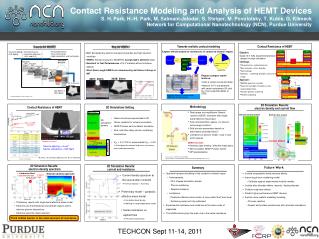
Contact Resistance Modeling and Analysis of HEMT Devices S. H. Park, H.-H. Park, M. Salmani-Jelodar, S. Steiger, M. Povolotsky, T. Kubis, G. Klimeck Network for Computational Nanotechnology (NCN), Purdue University. Virtual Source. E F. 0 nm. E F. E F. 2D simulation domain. E F.

E N D
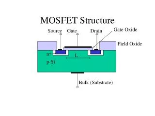
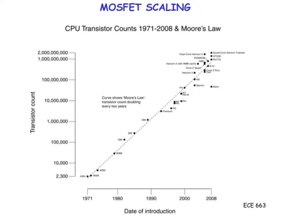
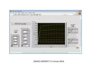
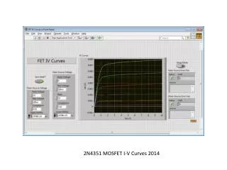
Contact Resistance Modeling and Analysis of HEMT DevicesS. H. Park, H.-H. Park, M. Salmani-Jelodar, S. Steiger, M. Povolotsky, T. Kubis, G. KlimeckNetwork for Computational Nanotechnology (NCN), Purdue University Virtual Source EF 0 nm EF EF 2D simulation domain EF In53Ga47As Plot Line In52Al48As Region of interest 90nm 100 nm InP In52Al48As EF Si δ-doping EF In53Ga47As InAs virtual drain In53Ga47As In52Al48As Towards III-V MOSFET Why III-V HEMTs? Towards realistic contact modeling Contact Resistance of HEMT • Device geometries • Channel materials • High-k dielectrics and metal gates • Strained channel • New gate dielectrics: • HfO2 and Al2O3 • Channel doping • S/D doping 40nm Explore effective parts for resistances in contact-to-channel region. • Objective: Guide III-V InAs experimental device design through simulation • Challenge: • 2D geometries, and confinement • New materials, strain, disorder • Gate leakage • Contacts – scattering, disorder, and curved shape. • Approach: • NEMO5 quantum simulator • Quantum transport simulations using realistic geometries • Includes phonon scattering • Parallel computing • III-V: Extraordinary electron transport properties and high injection velocities • HEMTs: Similar structure to MOSFETs except high-κ dielectric layer • Excellent to Test Performances of III-V material without interface defects • Short Gate Length HEMTs are Introduced by del Alamo’s Group at MIT Source Drain N+ Cap In0.53Ga0.47As N+ Cap In0.53Ga0.47As 2015-2019 Research In0.52Al0.48As In0.52Al0.48As Channel region Contact 1 Contact 2 InP InP Lead 1 channel Lead 2 Gate In0.52Al0.48As In0.52Al0.48As In0.52Al0.48As Contact-to-channel region channel In0.53Ga0.47As channel InAs Device Pie In0.53Ga0.47As In0.52Al0.48As III-V channel devices Simulation Domain Contact Pad • Regular compact model features: • Uses a virtual source and drain. • Need to fit I-V characteristic with series resistances (RS and RD) from experimentalists or ITRS 2008: 30nm Rpad 2007: 40nm N+ Cap InGaAs 35nm Rcap In0.52Al0.48As 15 nm Low-power & high-speed Y InP etch stop 6 nm In0.52Al0.48As X Rbarrier 11 nm Acknowledgement: Robert Chau, Intel 2 nm In0.53Ga0.47As Rside InAs 5 nm Virtual Drain 3 nm In0.53Ga0.47As Simulation domain of compact model (IEDM 2009, N. Kharche et al.) D.H. Kim et al., EDL 29, 830 (2008) In0.52Al0.48As 500nm 2D Simulation Results: electron density and current flow Methodology 2D Simulations Setting Contact Resistance of HEMT • Real-space non-equilibrium Green’s function (NEGF) formalism with single-band effective-mass basis • Self-consistent Born approx. for phonon self-energy functions1 • Bulk phonon parameters based on deformation potential theory2 • Limitations of phonon model : local in real and k spaces Electron density profile Electron flux vectors 25nm • Hetero-structures represented in 2D • Ohmic contacts for virtual source/drain • NEGF/Poisson self-consistent simulation • Intra- and inter-valley phonon scattering mechanisms • VDS = 0~0.15V for experimental VDD = 0.5V • Considered the channel and series resistances measured experimentally (a.u.) Corner effect • NEMO5 simulator: • Atomistic tight-binding / effective-mass basis • Self-consistent NEGF-Poisson Solver • MPI parallelization 0 Source spacing = 2 μm* Series resistance = 240 Ωμm [1] S. Jin et al., JAP 99, 123719 (2006) [2] M. Lundstrom, Fundamentals of carrier transport (Cambridge Univ. Press) *D.-H. Kim, J. D. A. del Alamo, IEEE Trans. Elec. Dev. 57, 1504 (2010) 2D Simulation Results: electron density spectrum 2D Simulation Results: current and resistance Future Work Summary • Quantum transport modeling of the contact-to-channel region • Achievements: - 2D L-shaped simulation domain • - Phonon scattering • - Resistive behavior • Limitations: - Parabolic effective-mass model over predict the Fermi level • - Scattering model not fully calibrated • Experimental resistance and model are at the same order of magnitude • The InAlAs barrier plays the main role in the series resistance • Include nonparabolic band structure effects • Improving phonon scattering model • – Calibrate against experimental mobility models • Include alloy disorder effects, impurity / doping disorder • Surface roughness effects • Predict higher performance HEMT devices • Explore more realistic modeling including: • Process variation • Dopant and surface randomness with atomistic simulations --- Conduction Band --- Electron Density Electron density spectrum • Current density spectrum at the source/drain contacts • Thermal injection + Tunneling δ-doped Layer InAlAs barrier n+ cap InGaAs (/cm3) • Preliminary model – parabolic effective-mass model • Conduction band too low • Working on nonparabolic band model n+ cap channel InAlAs • Preliminary results with single-band effective-mass model • Electrons are thermalized at source/drain regions due to electron-phonon interactions • Electrons pass the hetero-barriers InP InAlAs • Series resistance vs. applied bias • Resistive characteristic InGaAs InAs InGaAs InAlAs Thick InAlAs barrier is the main element of resistance TECHCON Sept 11-14, 2011