Download
1 / 16
160 likes | 362 Vues
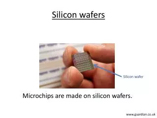
Automatic testing of Medipix wafers. Developing systems to measure Medipix chips Richard Plackett - CERN – April 2nd. Outline. The Medipix Project Hybrid Pixel Detectors The Medipix Chips ‘Real World’ Applications (and HEP) Automatic Wafer Testing Motivating Automatic Testing

E N D
Automatic testing of Medipix wafers Developing systems to measure Medipix chips Richard Plackett - CERN – April 2nd
Outline • The Medipix Project • Hybrid Pixel Detectors • The Medipix Chips • ‘Real World’ Applications (and HEP) • Automatic Wafer Testing • Motivating Automatic Testing • Tools Available • Using Optical Feedback • Giga-Pixel Chip Imaging • First Results • Next Steps • Further Work The newly arrived Medipix3 chips
Hybrid Pixel Detectors Hybrid Detectors are a ‘sandwich’ of a sensor and read-out chip. Each pixel can have its own analogue and digital elements.. Amplification, shaping, discrimination, counters etc. Very short connections to read-out reduce cross talk and noise. Sensor Bump-Bonding Amplification Medipix Project Discriminator & Counter Hybrid Detectors Medipix Chips Read-Out Applications Automatic Testing Motivation Tools Optical Feedback Chip Imaging First Results Next Steps Further Work High density solder bump bonding is a key technology
Medipix Chips Medipix1 (1997) Proof of concept, photon counting, 64x64 pixels, 3 bit threshold tuning 1um CMOS Medipix Project Hybrid Detectors Medipix Chips Medipix2 (2002) Photon counting , 55um pixels, 256x256, Positive and negative sensors, Pixel level leakage compensation, 3 side tile-able Upper and lower threshold levels 250nm CMOS Timepix (2006) As Medipix2, with additional.. Time over threshold energy measurement Accurate time of arrival count Applications Automatic Testing Motivation Tools Optical Feedback Chip Imaging First Results Next Steps Medipix3 (2009) 55um pixels, 256x256, charge sharing summation, 2 thresholds and 2 counters per pixel, quad pixel spectroscopic mode, continuous readout mode, 130nm CMOS Further Work
Modes of Operation Photon Counting Count hits over threshold rather than simply accumulating charge Available with all Medipix chips Time over Threshold Threshold Medipix Project Time over Threshold Measure the time a hit passes a threshold for a measurement of the energy deposited in the sensor. Hybrid Detectors Time of Arrival Medipix Chips Applications Time of Arrival Measure the time from a hit until the ‘shutter’ is closed Automatic Testing Motivation Shutter Tools Optical Feedback Spectroscopic Pixels Using 4 pixel ‘superpixels’ the many thresholds and counters give 8 levels of energy resolution whilst losing a factor of 2 spatial resolution Charge Summing If a ‘cluster’ of hits is found, allocate all the charge to the hardest hit pixel. This combats charge sharing. Chip Imaging First Results Next Steps Further Work
The Collaboration People are doing lots of things with Medipix chips Medipix CT The MARS project in NZ is making a ‘colour’ multi spectral CT scanner. Medipix Project Medipix XRD PANalytical (NL) is selling Medipix chips in its X-Ray Diffraction systems. Hybrid Detectors Medipix Chips Applications Automatic Testing Medipix in Space Will fly in 2010 as part of the LUCID cosmic ray flux experiment. Motivation Tools Optical Feedback Medipix to Mars Is being used in Houston to characterise Astronaut dosage for long term interplanetary missions. Chip Imaging First Results Next Steps Medipix Tomography Medipix is used in several high-res tomography studies with x-rays and neutrons at Erlangen, CTU an Bogotá. Further Work Medipix TPC Timepix was developed for use in next generation Time Projection Chambers, demonstrated by Freiburg.
More Collaborators Medipix Electron Microscopy Enhancing new electron microscopy systems in collaboration with Leiden & Cambridge. Medipix Photon Detectors New HPDs and Micro channel plate photon detectors from Glasgow and Berkley. Medipix Project Hybrid Detectors Medipix Chips Medipix at SLSs The Detector groups from ESRF and Diamond Synchrotron Light Sources are part of the collaboration. Applications Automatic Testing Motivation Tools Medipix in the LHC ATLAS and CMS are using Medipix chips as radiation monitoring devices providing real-time neutron monitoring. Optical Feedback Chip Imaging First Results Next Steps Medipix Mass Spectroscopy New generation imaging-spectroscopy systems at Kiev are using Medipix in fields such as proteomics. Further Work
Motivating Automatic Measurements • Medipix3 chips have a 32 bit serial number that must be burnt on, so *All* new chips have to pass through a probe station once. • For Medipix2/Timepix basic probing ~3 or 4 minutes per test so operators are continuously working for several hours to complete a wafer. • Currently each chip has to be positioned and contacted by hand which is VERY time consuming… (100 chips per wafer) • CERN is a production center and our collaborators rely on us to provide them with chips and assemblies. • For PANalytical a well controlled and characterised supply is commercially necessary Medipix Project Hybrid Detectors Medipix Chips Applications Automatic Testing Motivation Tools Optical Feedback Chip Imaging First Results Next Steps Further Work
Tools Available • SussMicroTec PA200 ‘semiautomatic’ probe station • Already used to for previous chips • Can be controlled via IP • Video feedback from microscope • Micron accuracy on chuck • Matlab • Training provided by ACEOLE • Easy image processing • Good control development libraries • Rapid development • Pixelman • Medipix Readout Software Medipix Project Hybrid Detectors Medipix Chips Applications Automatic Testing Motivation Tools Optical Feedback Chip Imaging Camera integrated into microscope provides an optical feedback First Results Next Steps Further Work Probe card powers and read out chips whilst still on the wafers 4 degree of freedom vacuum chuck provides accurate wafer positioning
Optical Feedback To trust the autonomous alignment and positioning we wanted some feedback . Using the video feed from the microscope camera.. • And the alignment marks on chips… • Then cross correlate … apply some cuts … peak finding … reducing multiple solutions… • We can have some confidence that the wafer is where we wanted it. • This approach allows us to be general – will work for all Medipix wafers and beyond. Medipix Project Hybrid Detectors Medipix Chips Applications Automatic Testing Motivation Medipix3 alignment marks Tools Medipix2 / Timepix alignment marks Optical Feedback Medipix1 ‘branding’ Chip Imaging First Results Next Steps Further Work
Example : Pad Finding Medipix Project Hybrid Detectors Medipix Chips Applications Automatic Testing Motivation Video feed Correlation Matrix Reference Tools Optical Feedback Chip Imaging First Results Next Steps Further Work Apply Probability Cuts Output Matrix
Giga-Pixel Chip Imaging Accurate positional control of the wafer lets us use the probe station as a giga-pixel camera to image the chip. Medipix Project Hybrid Detectors Medipix Chips Applications Automatic Testing Motivation Tools Optical Feedback Chip Imaging First Results Next Steps Further Work
Automatic Test Results • Currently able to test Medipix2 / Timepix • Probe positioning accurate to ~1um • Wafer alignment and mapping <20mins • Each chip is individually positioned with optical feedback and its location stored • Angular alignment to better than 0.01 degrees • Each chip tested in less than 1 minute • Analogue and Digital parts of the chip are tested • Voltage levels are optimised and saved • Has re-try capability to overcome bad contacts Medipix Project Hybrid Detectors Medipix Chips Applications Automatic Testing Motivation An action shot of the probe system Tools Optical Feedback Chip Imaging First Results Next Steps Further Work Wafer testing time has reduced from a day to 2 hours Operator only needed to start the system not run it continuously
Next Steps in System Development • Increasing Robustness and Finalising system • Introducing more checks into critical functions • Feedback from analysis routines to re-check chips if necessary • Automatically produce a wafer map when tests complete Medipix Project Hybrid Detectors Medipix Chips • Assembly Testing • 21 assemblies in one run • Individual optical alignment of assemblies ready • Different tests for each assembly easy to script • Individual probe height adjustment is still required Applications Automatic Testing Motivation Tools Optical Feedback Chip Imaging First Results • Medipix 3 – Testing and Identity Burning • System designed to work with multiple wafer types • Modular code means tests can be performed with minimal risk to wafers. • Need to be VERY careful with book-keeping. • Additional 3.3V voltage supply needs to be integrated. • Require Medipix3 readout system before we can start. Next Steps Further Work
Future Work • Characterising sensors at different temperatures • Work has begun preparing a cryostat, modified pieces have already been received from the workshop. • We plan to measure a series of sensors GaAs, CdTe, Si etc • We will also use it for ‘mechanical’ proving • Using XRD to analyze stresses in bonded assemblies • XRD Training provided at PAN as part of ACEOLE scheme • Will modify the PAN system to perform crystal stress measurements over the sensor surface. • Super-LHC Test-beams • Tests this summer to see if Medipix technology will be suitable for some upgrade proposals. • CERN @ School • I am working with the Langton Star Center, a secondary school project to help develop projects for a distributed cosmic ray detector based on the Timepix chip. • Initially 10 USB detectors will be sent to begin training staff in their operation. • GPS timing hardware has to be developed and integrated. • Links to the LUCID cosmic ray satellite project. Medipix Project Hybrid Detectors Medipix Chips Applications Automatic Testing Motivation Tools Optical Feedback Chip Imaging First Results Next Steps Further Work
Summary • The Medipix Chips are VERY versatile and the collaboration is active in many areas. • Need to automatically test chips by the wafer. • Has to be very reliable and accurate. • Wafers have been successfully tested automatically. • Enhancements for Medipix3 and assemblies in development. • Several other projects now beginning to take shape. ~Thank you for your attention~