Download
1 / 13
130 likes | 253 Vues
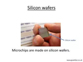
Medipix sensors included in MP wafers. Produced by Micron Semiconductor on n-in-p wafers (150 and 300 m m thick). To achieve good spatial resolution through efficient charge collection:. - HV performance (main focus in this work) - Optimal implant geometry. 2.

E N D
Medipix sensors included in MP wafers Produced by Micron Semiconductor on n-in-p wafers (150 and 300mm thick) To achieve good spatial resolution through efficient charge collection: - HV performance (main focus in this work) - Optimal implant geometry 2
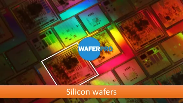
Pixel Detector Programme in Liverpool 6” wafers 2800-2825 fabricated by Micron Strip detectors: Polysilicon bias resistors Punch-through biasing Bias rail option Pixel detectors: FE-I3, FE-I4, PSI-46, MPIX-II, APC, APR (interleaved pixels) Pad detectors: RD-50, PSI, MPI guard structures, Cut edge scenarios (8, 4, 2, 1 rings) Test structures: Process control, device modelling in the double metal “n-in-p” FZ process 3
Pixel Detectors with Wire-bonded Readout Working horse: pixel sensors with interleaved readout implants connected to wire bond pads Pulse shape analysis Cross-calibration of ToT Fast “Cold” bonding to the readout for annealing studies Re-use of bonding pads No need to irradiate the readout -> good data quality Inter-”strip” resistance and capacitance measurements Measurement of the punch- through voltage of the biasing circuit Column-parallel / Row-parallel readout Shuffled R/O channels to minimise the cross talk between connection lines 4
Readout Implants, part I (resistances) Sheet resistance ~400 Ohm/square (implant dose ~1014 cm-2) Inter-”strip” resistance ~1 TOhm/cm for 50 um pitch (see spare slides) PCB for measurements of the punch through voltage, potentials on guard rings and characteristic inter-“strip” resistance and capacitance Sensor’s substrate is attached to the heat sink for cooling by the air flow 5
Readout Implants, part II (capacitances) Inter-”strip” capacitance ~0.5 pF/cm for 50 um pitch (see spare slides) Capacitance to bulk ~1 pF/sq. mm at full depletion voltage (reduces when the bias network is powered, this effect depends on the sensor size; it is not quantified here) IC(V) curves for the FE-I3 single chip sensors Full depletion voltage ~80 V (unirradiated, bulk resistivity ~15 kOhm.cm) 6
Readout Implants, part III (punch-through biasing) Atlas pixel sensor Punch-through gap = 3.5um Punch-through voltage ~1 V/um -> the hybrid designer should pay attention to: - potential of the bias ring connected to ASIC (pixel shortening, chip breakdown) - potential of the 1st GR connected to ASIC (chip breakdown) 7
Guard Structures “RD-50” “PSI” “MPI” “RD-50” I(V) curves for 4x4 mm2 pads “Floating metal” + more geometries (new wafer) 8
Measurements of the Guard Ring Potentials Measurement scheme 1: GR9 1 . . . GR1 GR2 GR3 GR2 GR1 GR4 GR9 2 . . . GR2 GR6 GR1 GR has a substrate potential unless bulk depletion reaches it Device modelling: guard structure is NOT a voltage divider ! 9
Interference with the Guard Structure Probe pads Alignment marks Straight implant and metal lines Straight implants, broken metal :-) :-) Thinned implants, metal bypass Thin and wide sections for pads :-( :-( I(V) curves for FE-I4 SC sensors I(V) curves for 4x4 mm2 pads 10
Cut Edge Studies RD-50 8x PSI 8x MPI 8x RD-50 guard structures 11 Breakdown condition: bulk depletion in the lateral direction reaches the cut edge
Charge Collection Measurements after High Radiation Doses Measurements for the Micron n-in-p strip detectors using a data acquisition system based on the SCTA-128VG readout chip (40 MHz readout speed) Detector thickness = 300+/-20 um A. Affolder, et. al., NIMA (2010) doi.10.1016/j.nima.2010.02.187 K. Hara, et. al., NIMA (2010) doi.10.1016/j.nima.2010.04.090 12
Spare Slide 5: new 6-inch Micron Pixel Wafer n-in-p, single metal FZ process, 300um 5x FE-I4 tiles (2guard ring options, 250 um and 450 um ) 14x FE-I4 SC (4 guard ring options, 450 um and 250 um) 12x FE-I3 SC (4 guard ring options, 40, 80, 200, 600 um) 2x Medipix-II tiles, 2x Medipix SC 4 diodes (process control, new GR) Test structures (transistor models, R, C, punch-through) Delivery: 14.09 (first batch) There is a room for 14x FE-I4 tiles (good homogeneity across the wafer) There are plans to deliver n-in-n, and thinned wafers and 1 wafer with no capacitor oxide
Proposal: making a Medipix only mask, to accommodate tiles, single sensors, variation of the GR structure to study effectiveness of asymmetric reduction of edge ..... Look for partners (I know interest from Prague) for sharing the mask cost. I propose production with Micron on 6” wafers (this can be added to the running program with CNM, with whom we can share ideas and test of new geometries.....).