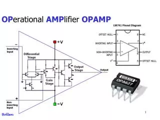
OpAmp Design
OpAmp Design. The design process involves two distinct activities: Architecture Design Find an architecture already available and adapt it to present requirements Create a new architecture that can meet requirements Component Design Determine transistor sizes

OpAmp Design
E N D
Presentation Transcript
OpAmpDesign The design process involves two distinct activities: • Architecture Design • Find an architecture already available and adapt it to present requirements • Create a new architecture that can meet requirements • Component Design • Determine transistor sizes • Determine biasing voltages/currents • Design compensation network
All op amps used as feedback amplifier: If not compensated well, closed-loop can be oscillatory or unstable. damping ratio z≈ phase margin PM / 100 Value of z: 1 0.7 0.6 0.5 0.4 0.3 Overshoot: 0 5% 10% 16% 25% 37% PM in deg: 70 60 50 40 30
UGF: frequency at which gain = 1 or 0 dB PM: phase margin = how much the phase is above critical (-180o) at UGF Closed-loop is unstable if PM < 0 UGF This is the loop-return gain when used in closed-loop. Only in buffer connection this is equal to O.L. gain. PM
UGF GM<0 p1 p2 z1 PM<0
UGF p1 p2
UGF GM p1 p2 z1 PM
Fully differential amplifiers • Have two loops: • DM feedback loop • CM feedback loop • DM loop closed by user, • don’t know feedback at design stage, • needs stability for all user feedback • CM loop closed by designer, • knows CMFB exactly, • but DM loop and CM loop share significant signal path, • needs stability for all user DM feedback
Half circuit for DM and half circuit for CM can be used to simplify analysis. Open loop gain can be analyzed to infer closed loop stability. Will focus on DM path transfer function
Types of Compensation • Miller - Use of a capacitor feeding back around a high-gain, inverting stage. • Miller capacitor only • Miller capacitor with an unity-gain buffer to block the forward path through the compensation capacitor. Can eliminate the RHP zero. • Miller with a nulling resistor. Similar to Miller but with an added series resistance to gain control over the RHP zero. • Self compensating - Load capacitor compensates the op amp (later). • Feedforward - Bypassing a positive gain amplifier resulting in phase lead. Gain can be less than unity.
Two stage Miller compensation Miller Effect v2 v1 i v2= AVv1 v1 i= v1/Z1 i= -v2/Z2 i = (v1-v2)/Zf = v1(1-AV)/Zf = v1/{Zf/(1-AV)} = - v2(1-1/AV)/Zf = - v2/{Zf/(1-1/AV)}
Nested Miller Compensation (NMC), Reverse Nested Miller Compensation (RNMC), Multipath Nested Miller Compensation (MNMC), Nested Gm-Cc Compensation (NGCC)
Active feedback frequency compensation (AFFC), Transconductancewith capacitance feedback frequency compensation (TCFC)
Single ended and differential have very similar Compensation needs Not quite VBP VBP I2 I1 Vo1 I2 Vo1 Vi Vo Vi- Vo Vi+ VBN I1 VBN
VBP VBP Vo1 CC CC Vi Vo Vi+ Vo+ Vo- Vi- Vb1 Vb1 VBN
If the first stage is cascode, the analysis stay similar VBP VBP VBPc Vo1 CC CC VBNc Vo Vo+ Vo- Vi Vi- Vi+ Vb1 Vb1 VBN Composite MOST with large ro
VDD Folded cascode same thing, except gm is from a different pair IN- IN+ CC CC Vo+ Vo-
Generic representative: VBP Vo1 Vi Vo Vb1
DC gain of first stage: AV1 = -gm1/(gds2+gds4)= -gm1/(I4(l2+ l4)) DC gain of second stage: AV2 = -gm6/(gds6+gds7)=- gm6/(I6(l6+ l7)) Total DC gain: gm1gm6 AV = (gds2+gds4)(gds6+gds7) gm1gm6 AV = I4I6 (l2+ l4)(l6+ l7) GBW = gm1/CC
Zf = 1/s(CC+Cgd6) ≈ 1/sCC When considering p1 (low freq), can ignore CL (including parasitics at vo): Therefore, AV6 = -gm6/(gds6+gds7) Z1eq = 1/sCC(1+ gm6/(gds6+gds7)) C1eq=CC(1+ gm6/(gds6+gds7))≈CCgm6/(gds6+gds7) -p1 ≈ w1 ≈ (gds2+gds4)/(C1+C1eq) ≈ (gds2+gds4)/(C1+CCgm6/(gds6+gds7)) ≈ (gds2+gds4)(gds6+gds7)/(CCgm6) Note: w1 decreases with increasing CC
M6 M7 CC C1 CL At frequencies much higher than w1, gds2 and gds4 can be viewed as open. Total go at vo: CC gds6+gds7+gm6 CC+C1 vo Total C at vo: C1CC CL+ CC+C1 -p2=w2= CCgm6+(C1+CC)(gds6+gds7) CL(C1+CC)+CCC1
gds6+gds7 Note that when CC=0, w2 = CL As CC is increased, w2 increases also. However, when CC is large, w2 does not increase as much with CC. w2 has a upper limit given by: gm6+gds6+gds7 gm6 ≈ CL+C1 CL+C1 When CC=C1, w2 ≈ (½gm6+gds6+gds7)/(CL+½C1) ≈ gm6/(2CL+C1) Hence, once CC is large, its main effect is to lower w1, and hence lower GBW.
Also note that, in contrast to single stage amplifiers for which increasing CL improves PM, for the two stage amplifier increasing CL actually reduces w2 and reduces PM. Hence, needs to design for max CL
There are two RHP zeros: z1 due to CC and M6 z1 = gm6/(CC+Cgd6) ≈ gm6/CC z2 due to Cgd2 and M2 z2 = gm2/Cgd2 >> z1 z1 significantly affects achievable GBW.
gm6/(CL+C1) f (I6) A0 z1≈ gm6/Cgd6 w1 w2 z2≈ gm2/Cgd2 -90 No PM -180
gm6/(CL+C1) f (I6) A0 z1≈ gm6/Cgd6 z2≈ gm2/Cgd2 w1 w2 z1≈ gm6/Cc -90 No PM -180
gm6/(CL+C1) f (I6) A0 w2 z1≈ gm6/CC w1 gm1/CC -90 PM -180
It is easy to see: PM ≈ 90o – tan-1(UGF/w2) – tan-1(UGF/z1) To have sufficient PM, need UGF < w2 and UGF << z1 In such case, UGF≈ GB ≈ gm1/CC = z1 * gm1/gm6. GB < w2 GB << z1 Hence, need: PM requirement decides how much lower: PM ≈ 90o – tan-1(GB/w2) – tan-1(GB/z1)
Possible design steps for max GB • For a given CL and Itot • Assume a current share ratio q, i.e. • I6+I5 = Itot, I5 = qI6 , I1 = I2 = I5/2 • Size W6, L6 to achieve max gm6/(CL+Cgs6) which is > w2 • C1 W6*L6, gm6 (W6/L6)0.5 • Size W1, L1 so that gm1≈ 0.1gm6 • this make z1 ≈ 10*GBW • Select CC to achieve required PM • by making gm1/CC < 0.5 w2 • Check slew rate: SR = I5/CC • Size M5, M7, M3/4 for current ratio, IMCR, etc
Comment • If we run the same total current Itot through a single stage common source amplifier made of M6 and M7 • Single pole go/CL • Gain gm6/go • Single stage amp GB = gm6/CL >gm6/(CL+C1) > w2 > gm1/CC = GB of two stage amp • Two stage amp achieves higher gain but speed is much slower! • Can the single stage speed be recovered?
Other considerations • Output slew rate: SR = I5/CC • Output swing range: VSS+Vdssat7 to VDD – Vdssat6 • Min ICM: VSS + Vdssat5 + VTN + Von1 • Max ICM: VDD - |VTP| - Von3 + VTN • Mirror node approx. pole/zero cancellation • Closed-loop pole stuck near by • Can cause slow settling
When vin is short, the D1 node sees a capacitance CM and a conductance of gm3 through the diode con. So: p3 = -gm3/CM When vin is float and vo=0. gm4 generate a current in id4=id2=id1. So the total conductance at D1 is gm3 + gm4. So: z3 = -(gm3+gm4)/CM =2*p3 If |p3| << GB, one closed-loop pole stuck nearby, causing slow settling!
Eliminating RHP Zero at gm6/CC icc = vg gm6 = CCdvCC/dt vg= RZCCdvCC/dt +vcc CCdvCC/dt (gm6RZ-1)CCdvCC/dt + gm6vcc=0
For the zero at M6 and CC, it becomes z1 = gm6/[CC(1-gm6Rz)] So, if Rz = 1/gm6, z1 → For such Rz, its effect on the p1 node can be ignored so p1 remains as before. Similarly, p2 does not change very much. similar design approach.
VDD M9 M8
VDD M9 M8
Another choice of Rz is to make z1 cancel w2: z1=gm6/CC(1-gm6Rz) ≈ - gm6/(CL+C1) CC+CL+C1 Rz = gm6CC CL+C1 1 (1+ ) = CC gm6
Let ID8 = aID6, size M6 and M8 so that VSG6 = VSG8 Then VSGz=VSG9 Assume Mz in triode Rz = bz(VSGz – |VT| - VSDz) ≈ bz(VSGz – |VT|) = bz(2ID8/b9)0.5 = bz(2aID6/b6)0.5(b6/b9)0.5 = bz/b6 *b6VON6 *(ab6/b9)0.5 = bz/b6 *1/gm6*(ab6/b9)0.5 Hence need: bz/b6 *(ab6/b9)0.5 =(CC+CL+C1)/CC
gm6/(CL+C1) f (I6) A0 -z1≈ w2 w1 gm1/CC -90 PM -180
With the same CC as before • Z1 cancels p2 • P3, z3, z2, not affected • P1 not affected much • Phase margin drop due to p2 and z1 nearly removed • Overall phase margin greatly improved • Effects of other poles and zero become more important • Can we reduce CC and improve GB?
A0 gm6/CL Operate not on this but on this or this z1≈ p2 z2≈ gm2/Cgd2 z4≈ gm6/Cgd6 w1 w2 pz=-1/RZCC -90 -180
Increasing GB by using smaller CC • It is possible to reduce CC to increase GB if z1/p2 pole zero cancellation is achieved • Can extend to gm6/CL • Or even a little bit higher • But cannot push up too much higher • Other poles, zeros • Imprecise mirror pole/zero cancellation • P2/z1 cancellation • GB cannot be too high relative to these p/z cancellation • Z2, z4, and pz=-1/RZCC must be much higher than GB
Possible design steps for max GB • For a given CL and Itot • Assume a current share ratio q, i.e. • I6+I5 = Itot, I5 = qI6 , I1 = I2 = I5/2 • Size W6, L6 to achieve max single stage GB1 = gm6/(CL+Coutpara) • A good trade off is to size W6 so that Cgs6 ≈ CL • If L_overlap ≈ 5% L6, this makes z4=gm6/Cgd6 ≈ 20*GB1 • Choose GB = aGB1, e.g. 0.5gm6/(CL+C1) • Choose CC to make p2 < GB, e.g. Cc=CL/4, p2 ≈ GB/1.5 • Size W1, L1 and adjust q so that gm1/CC ≈ GB • Make z2=gm2/Cgd2 > (10~20)GB, i.e. Cgd2 < 0.1Cc • Size Mz so that z1 cancels p2 • Make sure PM at f=GB is sufficient • Size other transistors so that para |p| > GB/(10~20) • Check slew rate, and size other transistors for ICMR, OSR, etc
If CL=C1=4Cc, -p2=gm6/(C1+CL+C1CL/Cc) =1/3 * gm6/(C1+CL) • -pz=1/RzCc, Rz=1/gm6 *(1+CL/Cc+C1/Cc); -pz=gm6/(Cc+C1+CL) ≈ 3*(-p2) • Pole/zero cancellation cancelled p2, but introduced a new pole pz at just a few times the p2 frequency, if done right;
For input common mode range • Vi+ = Vi- = Vicm should be allowed to vary over a large range without causing transistors to go triode • Vicm_max = (VDD – Vdssat_tail) – VT – Vdssat1 • Vicm_min = Vs of M1c – VT = VG of M1c/2c + Vdssat • VG of M1c must be low • But must be higher than Vo1 – VT1c • Room for Vo1 variation: +- VEB of 2nd stage
Hence, Vicm_min depends on differential signal • bias M1c adaptively, based on actual input signal
For Balanced Slew Rate • During output slewing • All of 1st stage current goes to Cc network • I-Rz drop ≈ constant • 2nd stage Vg variation << Vd or Vo • |Cc d(Vo-Vg)/dt| ≈ |Cc dVo/dt| <= |I1st st | • Slew rate = max |dVo/dt| = I1st st /Cc • On the otherhand • I2nd st bias - I1st st is to charge CL+Cdbs • max |dVo/dt| = (I2nd st bias - I1st st )/(CL+Cdbs) • Want (I2nd st bias - I1st st )/(CL+Cdbs) = I1st st /Cc • I2nd st drive max - I1st st is to discharge CL+Cdbs