Download
1 / 28
280 likes | 488 Vues
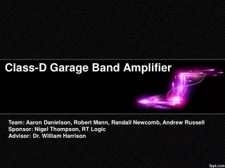
Class-D Garage Band Amplifier. Team: Aaron Danielson, Robert Mann, Randall Newcomb, Andrew Russell Sponsor: Nigel Thompson, RT Logic Advisor: Dr. William Harrison. Overview. Purpose of the Class-D Garage Band Amplifier Versus Commercial Products System Concept System Block Diagram

E N D
Class-D Garage Band Amplifier Team: Aaron Danielson, Robert Mann, Randall Newcomb, Andrew Russell Sponsor: Nigel Thompson, RT Logic Advisor: Dr. William Harrison
Overview • Purpose of the Class-D Garage Band Amplifier • Versus Commercial Products • System Concept • System Block Diagram • Major Tasks • Stretch Goals • Digital Signal Processor • Budget Overview • Project Schedule
Purpose • Class D Amplifier Power Efficiency • Price Point • Customizability • Open Source
Major Tasks - FPGA • Top Level Wrapper - Randy • Contains all the modules for testing that will be synthesized onto the FPGA. • Digital Signal Processor - Aaron • Design 4 filters – two each for bass & treble. • Interface with menu HSM to allow user to adjust settings. • Hardware State Machine - Rob • Implement a menu to control all the systems (LCD, ADC, DAC, DSP, SIGGEN, USER INPUT)
Major Tasks – Output Stage • Amplifier Output Stage - Andrew • Order and solder breakout boards • Surface mount pin packages (64 pin) • Used for initial testing of components • Layout custom PCB • 4 layer for power handling capability • Implement final design and test the output stage
Stretch Goals • An all digital amplifier will be implemented • No analog signals between input and speaker out • Add sound effects to the DSP • Echo • Reverb • Vacuum tube emulation • Speaker Enclosure • Build the enclosure • Design bandpass filters for the selected speaker
Printed Circuit Board (PCB) • 4 Layer PCB • Gives full ground and power planes • Necessary for high power circuits • Qualities/Needs outweigh the cost Signal Ground Power 12V 50V Signal
PCB Ground • Analog and Digital GND
PCB Power • Split Planes • Half-Bridge Power (+50V) • Regulators, Other Circuitry (+12V)
Noise • PWM amplifier switching • Analog and Digital ground shorted • Crosstalk • Power Supply • How to deal with it • Decoupling Capacitors • Maximize distance between traces • Proper component selection
Conclusion • Minimal Cost Versus Commercial Products • Design Implementation • Stretch Goals if Time Permits • Budget Situation • Task Scheduling and Project Progress