BJT in Saturation Mode
BJT in Saturation Mode. Section 4.5. Review of BJT in the active Region BJT in Saturation Mode Digital Integrated Circuits. BJT In the Active Region. Electrons are injected into the BC junction. Electrons are injected into the B; holes to the E. Electrons are swept across

BJT in Saturation Mode
E N D
Presentation Transcript
BJT in Saturation Mode Section 4.5
Review of BJT in the active Region • BJT in Saturation Mode • Digital Integrated Circuits
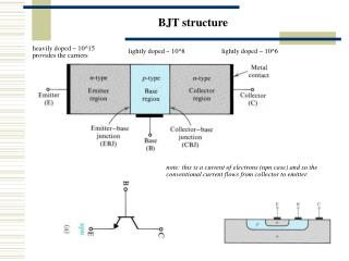
BJT In the Active Region Electrons are injected into the BC junction Electrons are injected into the B; holes to the E. Electrons are swept across the reversed biased BC
Useful Equations β: typically 100-200. Base current is amplified! Apply KCL to the transistor.
BJT in Saturation Mode Key assumption so far: BE=Forward Biased BC=Reverse Biased What happens when these assumptions are not true?
Review: Forward Bias Diode E Depletion region shrinks due to charges from the battery. The electric field is weaker. Majority carrier can cross the junction via diffusion; Greater diffusion current. Current flows from P side to N side
Review: PN Junction under Reverse Bias Reverse: Connect the + terminal to the n side. Depletion region widens. Therefore, stronger E. Minority carrier to cross the PN junction easily through diffusion. Current is composed mostly of drift current contributed by minority carriers. np to the left and pn to the right. Current from n side to p side, the current is negative. E
Hole Current into the Collector A reverse biased BCJ keeps holes in the base. But as BCJ becomes forward biased, the strong electric field which opposes of the movement of holes into the collector is weakened. There is now a hole current into the collector. Net Result: heavy saturation leads to a sharp rise in the base current and a rapid fall in β.
Energy Band Diagram of a Reverse Biased PN Junction np P N pn np P N Stronger E field in the depletion region pn
A Large Signal Model of the BJT The net collector current decreases as the collector enter into saturation
General Rules • As a rule of thumb, we permit soft saturation with VBC <400 mV because the current in the B-C junction is negligible, provided that various tolerances in the component values do not drive the device into deep saturation. • For a device in soft saturation or active region, we approximate IC as Isexp(VBE/VT) • In the deep saturation region, the collector-emitter voltage approaches a constant value called VCE, SAT (about 200 mV).
Use Transistor in Simulation (Error!, put 2n3904 here!)
BJT Inverter (Define the input voltage as a variable)
RTL (Resistor-Transistor Logic) Vout VA VB First introduced in 1962! (50 years ago!) What is the logic function?
RTL Based NOR NOR is an universal gate! If you can build a NOR, you can build any logic.
Diode-Transistor Logic What is the logic function? This resistor allow charges to be drained from the base
Sweep VB VS: the input voltage at which the output is approximately 2V. VS~2V Condition: VA=4V, VC=4V. VB is swept from 0 to 4V
Diode-Transistor Logic This resistor allow charges to be drained from the base
Sweep VB Fixed VA=4V VCC=4V Sweep VB from 0 to 4 V Increase the VS by about one diode drop.
Basic TTL Gate Diode is replaced by TTL A “relative “ of 7400LS Gate
Sweep VB Fixed VA=4V VCC=4V Sweep VB from 0 to 4 V
7400 NAND Gate 7400 Schematic We will revisit this schematic in a couple of weeks!