Download
1 / 27
270 likes | 716 Vues
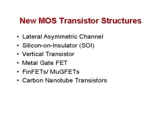
Lateral Asymmetric Channel (LAC) Transistors. Asymmetrically doped channel; heavier doping near source Improved characteristics Better DIBL Velocity overshoot Improved hot-carrier performance Disadvantage: Design difficult. Fabrication - LAC Transistors.

E N D
Lateral Asymmetric Channel (LAC) Transistors • Asymmetrically doped channel; heavier doping near source • Improved characteristics • Better DIBL • Velocity overshoot • Improved hot-carrier performance • Disadvantage: Design difficult
Fabrication - LAC Transistors • E-beam lithography used to define channel lengths down to 100 nm • VT implant (tilted by 7-15 degrees) for LAC devices done after gate oxidation • Two-step Ti silicidation and Ge preamorphization to control silicide depth and reduce series resistance
Silicon-on-Insulator (SOI) • Active silicon on a thick insulator (SiO2) • Mainstream technology of the future?
SOI-Advantages • Higher Driving Current: Due to the floating body effect, the "off" threshold voltage becomes higher, while the "on" threshold voltage becomes lower. Subthreshold slope improves and leads to a possibility of scaling the power supply down. Additionally it creates the low static power consumption. • Reduction of Parasitic Capacitance: Because the substrate is floating, the Source & Drain capacitance of the transistor is eliminated resulting in the improvements of speed. It also contributes the lower dynamic power consumption and higher clock frequency. • No Body Effect • Latch-up Immunity: Due to the floating substrate, possibly generated hot carriers do not go through the substrate preventing the substrate voltage from rising up enough to form the forward junction between source and body. • Improved Density • Noise Decoupling
SOI Disadvantages Identical process flow for PD-SOI However, its FBE(Floating-Body Effect) imposes a considerable difficulty in circuit and device design ex: “Kink Effect in PD-SOI” Single Transistor Latch-Up.
Metal Gate FET • Why not Poly-Si ? • Poly Depletion (insufficient activation) • Boron Penetration (ultra-thin oxides) • High-K Dielectrics (incompatible) • VT adjustment (with jms)
Vertical Replacement Gate Transistor From J. M. Hergenrother et al., IEDM 1999, p.75
Metal Gate FET • Why not Poly-Si ? • Poly Depletion (insufficient activation) • Boron Penetration (ultra-thin oxides) • High-K Dielectrics (incompatible) • VT adjustment (with jms)
FinFET – A 3-D MOSFET • Vertical Channels • Double Gate • SOI • Better Performance
Double & Triple Gate FinFETs Triple Gate FinFET: 20 % greater currents Double Gate FinFET
Contacting Finfets UC Berkeley
Finfet S/D contact Design T.J.King, UC Berkeley
Litho- FinFET process flow • Makes use of SOI Delta structure on planar technology • Gate first process • As tsi < Lg, e-beam or opt. lithography with extensive line width trimming used • Fabrication steps after fin formation are analogous to Bulk MOS
Spacer FinFET • Sub litho dimensions can be achieved • Fin quality determined by surface roughness • Methods for fine fins are to be developed. • Fin pitch should be smaller than Fin height
FinFET circuit prospects • Useful for driving I/C dominated lines such as WL/BL in SRAM, Registers, DRAM • 70% of chip area/leakage by these blocks in uP • In FinFET ION increased without area/leakage penalty • Also we can afford decrease in VDD and increase in Vt, saving power for same performance. • Optimum (VDD – TSi – VT ) design space required for FinFET chips. (as fin aspect ratio is typically 5)
FinFET circuit prospects • Independent Double-Gate MOSFETs • Front and back (top or bottom) gates can operate independently • Better logic design • Dynamic VT control, and thus adaptive threshold • and leakage tuning. • Mixer Circuits for RF applications • M1 and M2 can be combined into one DGFET • Switch level model for conduction is controlled using signal ‘A OR B’ • One of the advantages of planar double-gate devices over FinFETs from a • circuit designer’s perspective is the possibility of independent back-gate-bias.
FinFET circuit prospects IEEE Transactions on Electron Devices, 2005.
Carbon Nanotubes Graphene sheet Single wall CNT Multi wall CNT CNT’s can be single-wall or multi-wall CNT diameter can range from 1 – 20 nm CNT lengths can range from 100 nm – 10 um CNT’s can be semiconducting or metallic CNT’s can be used as FETs, interconnects, ….
Carbon Nanotube Transistor CNT Field Effect Transistor
Conclusions • MOS transistors are conceptually simple devices • Both NMOS and PMOS transistors can be made, and effectively combined in CMOS circuits • Transistor scaling leads to great benefits, and has driven Moore’s law during the last three decades • Transistor down-scaling leads to some problems, which have been effectively combated by improved transistor design • Scaling is likely to continue till at least 2010, when transistor dimensions will be less than 0.05μm