Download
1 / 1
10 likes | 222 Vues
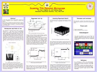
(a). (b). (c). Scanning THz Emission Microscope. Tao Yuan, Jingzhou Xu , and Xicheng Zhang Rensselaer Polytechnic Institute, Troy, New York . Abstract A THz image system with very high spatial resolution will provide an important tool for research of material local property.

E N D
(a) (b) (c) Scanning THz Emission Microscope Tao Yuan,Jingzhou Xu, and Xicheng Zhang Rensselaer Polytechnic Institute, Troy, New York Abstract A THz image system with very high spatial resolution will provide an important tool for research of material local property. Here we report a scanning THz emission microscope. Using the near field technology, the microscope has a lateral resolution of 1 nanometer, which corresponds to a resolution/wave-length ratio of order of 10-6. Scanning Experiment Result Experiment Set Up Discussion and conclusion We also put the tip on a 3-D piezo driving stage so that we can do a 3-D scan to demonstrate the resolution of the system. We have built a scanning THz emission Microscope and demonstrated its nanoscale resolution and 2D image scanning ability. • Future work • Improve scanning speed. • Improve the position control of the tip. • Acknowledgment • This work was supported in part by the Center for Subsurface Sensing and Imaging Systems, under the Engineering Research Centers Program of the National Science Foundation. The project fits in level 1 Fundamental Science. R1. Introduction and State of Art The resolution of conventional image system is limited by diffraction: x /NA, which is the so called Rayleigh Criterion. The limitation is more serious for THz image system because of the long wavelength used (~300 m for 1THz). Sub-wavelength resolution can be achieved by near field technology shown in figure 1 (b) and (c), which are sub-wavelength aperture and aperture-less method. In aperture-less method, a very sharp metal tip is put very close to the sample surface so that it scatters the evanescent wave from the surface to the far field for detection. In this way, the resolution is determined by the tip end size. The best resolution achieved by optical near field microscope is 1 nm [1]. Fig.2, A schematic graph of the experimental setup However in these two setups, the signal intensity or contrast is usually very small. To break through the bottle neck, we proposed a scanning THz emission microscope. Figure 2 shows schematic of our setup. An ultrafast near infrared laser pulse is shining onto the interface of a STM tip and semiconductor sample. An AC voltage is applied between the tip and semiconductor. The AC voltage produces an electrical field between the tip and the sample, which modulates the THz pulse generated by the laser pulse. Detection of this modulation gives the THz signal of the tip. Now the interface works as a THz source, which has a very small size, since it is determined by the tip end size. A’ Fig. 4, THz 2-D image of a gold grating on p-InAs wafer. Figure 4 shows the THz 2-D image of a metal grating structure on p-InAs. The flat parts reflect the metal line, which is 6 m wide in the 10 m grating period. The scanning region is 40 40 m with scanning step 0.1 m and 0.5 m in Y and X direction respectively. A Reference Fig. 3. THz signal and Tip current signal measured at the same time as tip approaches the sample. Fig. 5. The peak value of THz signal as tip scanning across a metal film edge on p-InAs wafer. [1] F. Zenhausern, Y. Martin, H.K. Wickramasinghe, “Scanning interferometric apertureless microscopy: Optical imaging at 10 angstrom resolution”, Science,269, 1083 (1995). [2] K.L. Wang, A. Barkan, D.M. Mittleman, CMP5, The Conderence of Laser and Electro-Optics (CLEO), (2003). [3] H.-T. Chen, R. Kersting, G. Cho, “Terahertz Imaging with nanometer resolution”, OpAppl. Phys. Lett., Vol. 83, 3009 (2003) Fig. 1, Rayleigh criterion and Near field method THz near field microscope have been developed by several groups. In their setup, the small particle is the end of a sharp tip. The scattered signal can be detected[2]. Another way is to detect transmitted THz signal and the difference between incident and transmitted THz signal resulted from the sum of absorption and scattering[3]. Sub micron resolution has been reported. Contact: zhangxc@rpi.edu Figure 5 shows the THz peak signal as the tip scanning across the edge of a Cr-Au film ( average 25 nm thick) on a 1 X 1016 cm-3 doping p-type InAs wafer, The metal film thickness changes gradually to 0 at the edge. While on the metal side, there is no tip THz signal. The transition from the wafer side, which has tip THz signal, to the metal side is 1 step (1 nm). This implies a lateral resolution of no more than 1 nm. Figure 3 shows that the tip current and THz signal appear exactly the same time as the tip approaches the sample surface. The 10% to 90% transition range is within 1 nm, demonstrating a vertical resolution of around 1 nm. This shows a similar property to STM.