Download
1 / 35
350 likes | 520 Vues
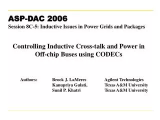
ASP-DAC 2006 Session 8C-5: Inductive Issues in Power Grids and Packages. Controlling Inductive Cross-talk and Power in Off-chip Buses using CODECs. Authors: Brock J. LaMeres Agilent Technologies Kanupriya Gulati, Texas A&M University Sunil P. Khatri Texas A&M University.

E N D
ASP-DAC 2006Session 8C-5: Inductive Issues in Power Grids and Packages Controlling Inductive Cross-talk and Power in Off-chip Buses using CODECs Authors: Brock J. LaMeres Agilent Technologies Kanupriya Gulati, Texas A&M University Sunil P. Khatri Texas A&M University
Motivation • Power delivery is the biggest challenge facing designers entering DSM - The IC core current continues to increases (P4 = 80Amps). - The package interconnect inductance limits instantaneous current delivery. - The inductance leads to ground and power supply bounce. • SSN on signal pins is the leading cause of inter-chip bus failure - Ground/power supply bounce causes unwanted switching. - Mutual Inductive cross-talk causes edge degradation which limits speed. - Mutual Inductive cross-talk causes glitches which results in unwanted switching. Further, power in off-chip buses can be significant. - Large percentage of power may be consumed in the output stages • Aggressive package design helps, but is too expensive: - Flip-Chip technology can reduce the interconnect inductance. - Flip-Chip requires a unique package design for each ASIC. - This leads to longer process time which equals cost. - 90% of ASIC design starts use wire-bonding due to its low cost. - Wire-bonding has large parasitic inductance that must be addressed.
Our Solution “Encode Off-Chip Data to Avoid Inductive Cross-talk & Power Consumption” • Avoid the following cases: 1) Excessive switching in the same direction = reduce ground/power bounce 2) Excessive X-talk on a signal when switching = reduce edge degradation 3) Excessive X-talk on signal when static = reduce glitching 4) At the same time, limit the number of transitions = reduce power
Our Solution • This results in: 1) A subset of vectors is transmitted that avoids inductive X-talk & power. 2) The off-chip bus can now be ran at a higher data rate.3)The subset of vectors running faster can achieve a higher throughput over the original set of vectors running slower. Throughput Throughput of less vectors of more vectors at higher data-rate at lower data-rate
Agenda 1) Inductive X-talk & Power 2) Terminology 3) Methodology 4) Experimental Results 5) Conclusion
1) Inductive X-Talk Supply Bounce The instantaneous current that flows when signals switch induces a voltage across the inductance of the power supply interconnect following: When more than one signal returns current through one supply pin, the expression becomes: NOTE: Reducing the number of signals switching in the same direction at the same time will reduce the supply bounce.
1) Inductive X-Talk Glitching Mutual inductive coupling from neighboring signals that are switching cause a voltage to induce on the victim that is static: The net coupling is the summation from all neighboring signals that are switching: NOTE: The mutual inductive coupling can be canceled out when two neighbors of equal Kik switch in opposite directions. Also, Kik is the mutual inductive coupling coefficient
1) Inductive X-Talk Edge Degradation Mutual inductive coupling from neighboring signals that are switching cause a voltage to be induced on the victim that is also switching. This follows the same expression as glitch coupling: The mutual inductive coupling can be manipulated to cause a positive (negative) glitch for a rising (falling) signal. Mutual coupling can thus be exploited so as to help the transition resulting in a faster rise-time or fall-time (alternately, to not hinder the risetime of the transition)
1) Power Power Consumption The power consumed in the output stage is proportional to the capacitance being driven, the output voltage swing, and the switching frequency. NOTE: Power is proportional to the number of switching pins.
2) Terminology Define the following:n = width of the bus segment where each bus segment consists of n-2 signals and 1 VDD and 1 VSS.j = the segment consisting of an n-bit bus.j is the segment under consideration.j-1 is the segment to the immediate left.j+1 is the segment to the immediate right. each segment has the same VDD/VSS placement.
2) Terminology Define the following: = the transition (vector sequence) that the ith signal in the jth segment is undergoing, where = 1 = rising edge= -1 = falling edge = 0 = signal is static This 3-valued algebra enables us to model mutual inductive coupling of any sign
2) Terminology Define the following coding constraints:Supply Bounce if is a supply pin, the total bounce on this pin is bounded by Pbnc.Pbnc is a user defined constant. Glitching if is a signal pin and is static (= 0), the total magnitude of the glitch from switching neighbors should be less than P0 . P0 is a user defined constant. Edge Degradationif is a signal pin and is switching (= 1/-1), the total magnitude of the coupling from switching neighbors should be greater than P1 / P-1. This coupling should not hurt (should aid)the transition. P1 / P-1 is a user defined constant.
2) Terminology - Power Define the following coding constraints: Power for a given segment j, the total power consumption on that segment is bounded by Ppower.Ppower is a user defined constant.
2) Terminology Also define the following: p = how far away to consider coupling (ex., p = 3, consider K11, K12, and K13on each side of the victim) kq = Magnitude of coupled voltage on pin i when its qth neighbor p switches:
3) Methodology For each pin vij within segment j, we will write a series of constraints that will bound the inductive cross-talk magnitude. The constraints will differ depending on whether vij is a signal or power pin. The coupling constraints will consider signals in adjacent segments (j+1, j-1) depending on p.
0 0 0 0 3) Methodology – Signal Pin Constraints Glitching : coupling is bounded by P0 Example: v2j =0, and p=3. This means the three adjacent neighbors on either side of v2j need to be considered (v4j-1, v0j, v1j, v3j, v4j, v0j+1).Note we use modulo n arithmetic (and consider adjacent segments as required). v2j = 0 (static) -P0<k3·(v4j-1) + k2·(v0j ) + k1·(v1j) + k1·(v3j) + k2·(v4j) + k3·(v0j+1) <P0 The constraint equation is tested against each possible transition and the transitions that violate the constraint are eliminated.
0 0 0 0 0 0 0 0 3) Methodology – Signal Pin Constraints Edge Degradation : coupling is bounded by P1and P-1 Example: v2j = 1 or -1, and p = 3. This means the three adjacent neighbors on either side of v2j need to be considered (v4j-1, v0j, v1j, v3j, v4j, v0j+1).v2j = 1 (rising) k3·(v4j-1) + k2·(v0j ) + k1·(v1j) + k1·(v3j) + k2·(v4j) + k3·(v0j+1) >P1 v2j = -1 (falling) k3·(v4j-1) + k2·(v0j ) + k1·(v1j) + k1·(v3j) + k2·(v4j) + k3·(v0j+1) <P-1 Again, the constraint equations are tested against each possible transition and the transitions that violate the constraints are eliminated.
3) Methodology – Power Pin Constraints Supply Bounce : coupling is bounded by Pbnc Example: v0j =VDD or VSS. The total number of switching signals that use v0j to return current must be considered. Due to symmetry of the bus arrangement, signal pins will always return current through two supply pins. i.e., (v0j-1 and v0j) or(v4j and v4j+1). This results in the self inductance of the return path being divided by 2. Let z = |L di/dt| for any pin. Then, v0j = VDD (z/2)·(# of vij pins that are 1) <Pbnc v4j = VSS (z/2)·(# of vij pins that are -1) <Pbnc
3) Methodology – Power Constraints Power Consumption : consumption is bounded by Ppower Example: For segment j. The total number of switching signals can be constrained to reduce power. Segment j (# of vij pins that are 1 or -1) <Ppower
3) Methodology – Constructing Legal Vectors Sequences • For each bit in the jth segment bus, constraints are written. • If the pin is a signal, 3 constraint equations are written; - v0j = 0, the bit is static and a glitching constraint is written - v0j = 1, the bit is rising and an edge degradation constraint is written. - v0j = -1, the bit is falling and an edge degradation constraint is written. • If the pin is VDD, 1 constraint equation is written to avoid supply bounce. • If the pin is VSS, 1 constraint equation is written to avoid ground bounce. • For the segment, 1 constraint equation is written to constrain power.
3) Methodology – Constructing Legal Vectors Sequences • This results in the total number of constraint equations written is: • (3·n – 3) • Each equation must be evaluated for each possible transition to verify if the transition meets the constraints. The total number of transitions that are evaluated depends on n and p: • 3(n+2p – 6) • This follows since there are n-2 signal pins in the segment j, and 2p-4 signal pins in neighboring segments. • The values of n and p are small in practice, hence this is tractable.
3) Methodology – Constructing the CODEC The remaining legal transitions are used to create the CODEC. The total number of remaining legal transitions will depend on how aggressive the user-defined constants are chosen (P0, P1, P-1, Pbnc, Ppower) From the remaining legal transitions, find the effective bus width m that can be encoded using a physical bus of width n, using a memory-based CODEC. Utilize a fixpoint computation
3) Methodology – Constructing the CODEC 000 101 001 010 011 Represent remaining legal transitions in a digraph Algorithm to find CODEC: Let n = size of physical bus Let m = size of effective bus Then the digraph of legal transitions of the n bit bus can encode an m bit bus (m < n) iff We can find a closed set S of nodes such that |S| ≥ 2m Each vertex s in S has at least 2m out-edges (including self-edges) to vertices s’ in S Now we can synthesize the encoder and decoder (memory based). 110 100 111
4) Experimental Results – 5 Signal Pins Example Bus: n=7, p=2 P0, P1, P-1, Pbnc Aggressive Encoding 5% of VDDNon-Aggressive Encoding 12.5% of VDDPower Encoding 20% of Max
4) Experimental Results – Constraint Equations # of Constraints = (3n – 3) = 121) v0j = VDD(L/2)· (# of vij pins that are 1) < Pbnc2) v1j = 1k1· (v2j) + k2· (v3j) > P13) v1j = -1k1· (v2j) + k2· (v3j) < P-14) v1j = 0- P0< k1· (v2j) + k2· (v3j) < P05) v2j = 1k1· (v1j) + k1· (v3j) > P16) v2j = -1k1· (v1j) + k1· (v3j) < P-17) v2j = 0- P0< k1· (v1j) + k1· (v3j) < P08) v3j = 1k2· (v1j) + k1· (v2j) > P19) v3j = -1k2· (v1j) + k1· (v2j) < P-110) v3j = 0- P0< k2· (v1j) + k1· (v2j) < P011) v4j = VSS(L/2)· (# of vij pins that are -1) < Pbnc12) (# of vij pins that are -1 or 1) < Ppower
4) Experimental Results – CASE 1: Fixed di/dt Rule(s) ViolatedTransitionAggressiveNon Aggressive 011 violates 1,4 - 0-1-1 violates 4,11 - 101 violates 1,7 - 110 violates 1,10 - 111 violates 1,2,5,8 violates 11 11-1 violates 1 - 1-11 violates 1 - 1-1-1 violates 11 - -10-1 violates 7,11 - -111 violates 1 - -11-1 violates 11 - -1-10 violates 10,11 - -1-11 violates 11 - -1-1-1 violates 3,6,9,11 violates 1 Transitions Eliminated due to Rule Violations
4) Experimental Results – CASE 1: Fixed di/dt Overhead = 1 - Effective = n - m Physical m Encoded data avoids Inductive X-talk pattern Bus can be ran faster
4) Experimental Results – CASE 1: Fixed di/dt Ground Bounce Simulation
4) Experimental Results – CASE 1: Fixed di/dt Glitch Simulation
4) Experimental Results – CASE 1: Fixed di/dt Edge Degradation Simulation
4) Experimental Results – CASE 2: Variable di/dt di/dt was swept for both the non-encoded and encoded configuration. the maximum di/dt was recorded that resulted in a failure. Failure : 5% of VDD (Aggressive) and 12.5% of VDD (Non-Aggressive) the maximum di/dt was converted to data rate and throughput. Original Aggressive Non-Aggr Maximum di/dt: 8 MA/s 19.9 MA/s 37 MA/s Maximum data-rate per pin: 133 Mb/s 333 Mb/s 667 Mb/s Effective bus width: 5 4 2 Total Throughput: 667 Mb/s 1332 Mb/s 1332 Mb/s Improvement - 100%100% Power Constraint (% of Max) 100% 20% 20%
4) Experimental Results – ASIC Synthesis A 0.13um, TSMC ASIC process was used. Delay and Area Extracted
4) Experimental Results – FPGA Implementation A Xilinx, Virtex-II, 0.35um, FPGA was used. Delay and Area Extracted
5) Conclusion Using a single mathematical framework, inductive X-talk & power constraints can be written that consider supply bounce, glitching, and edge degradation. This technique can be used to encode off-chip data transmission to reduce inductive X-talk & power to acceptable levels. It was demonstrated that even after reducing the effective bus size, the improvement in per pin data-rate resulted in an increasein throughput compared to a non-encoded bus.