
RC Circuits and Capacitor Charging Effects
E N D
Presentation Transcript
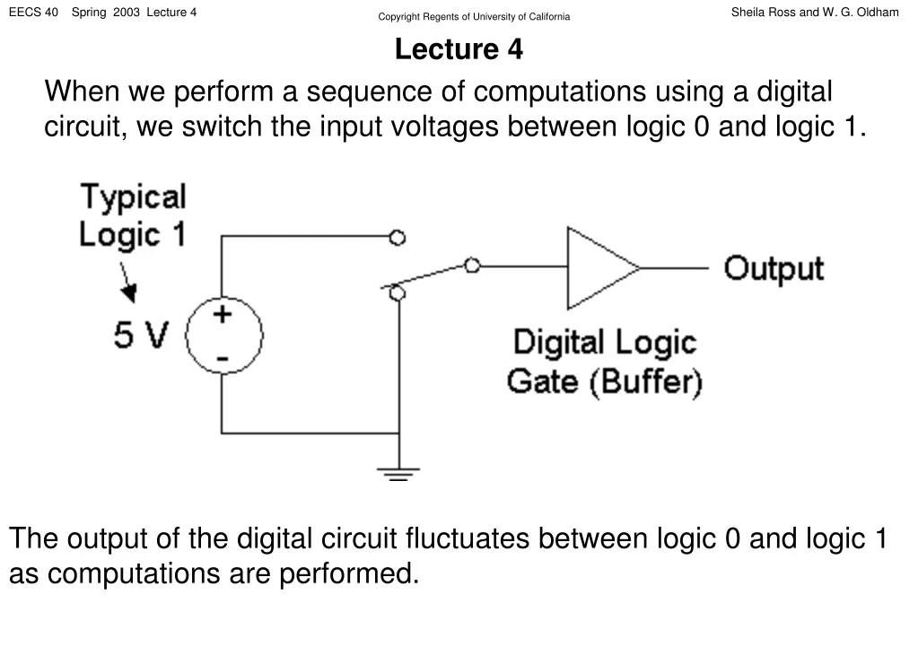
Lecture 4 When we perform a sequence of computations using a digital circuit, we switch the input voltages between logic 0 and logic 1. The output of the digital circuit fluctuates between logic 0 and logic 1 as computations are performed.
Every node in a circuit has capacitance to ground, and it’s the charging of these capacitances that limits real circuit performance (speed) voltage time voltage time RC Circuits We compute with pulses We send beautiful pulses in But we receive lousy-looking pulses at the output Capacitor charging effects are responsible!
RC Response R Internal Model of Logic Gate V V out in C Behavior of Vout after change in Vin Vout Vout Vin Vout(t=0) Vout(t=0) Vin 0 0 time 0 time 0
KCL: (Vin – Vout) / R = C dVout / dt RC Response Derivation R KCL at node “out”: out + + Current into “out” from the left: Vout Vin C _ (Vin - Vout) / R - ground Current out of “out” down to ground: C dVout / dt “Time Constant” t = RC Vout(t) = Vin + [ Vout(t=0) – Vin ] e-t/(RC) Solution:
Charging and Discharging Vout(t) = Vin(1-e-t/t) + Vout(t=0)e-t/t Discharging: Vin < Vout(t=0) Charging: Vin > Vout(t=0) Vout Vout Vin Vout(t=0) .63 Vin+ .37 Vout(t=0) .63 Vin+ .37 Vout(t=0) Vout(t=0) Vin 0 0 t t time time 63% of transition complete after 1 t
Vout Vout V1 V1 .63 V1 .37 V1 0 0 time 0 time t 0 t Common Cases Transition from logic 0 to logic 1 (charging) Transition from logic 1 to logic 0 (discharging) Vout(t) = V1e-t/t Vout(t) = V1(1-e-t/t) (V1 is logic 1 voltage)
R Input node Output node Vout + C Vin - ground Charging and discharging in RC Circuits(The official EE40 Easy Method) Method of solving for any node voltage in a single capacitor circuit. 1) Simplify the circuit so it looks like one resistor, a source, and a capacitor (it will take another two weeks to learn all the tricks to do this.) But then the circuit looks like this: 2) The time constant is t = RC. 3) Solve for the capacitor voltage before the transient, Vout(t=0). 4) Solve the for asymptotic value of capacitor voltage. Hint: Capacitor eventually conducts no current (dV/dt dies out asymptotically). 5) Sketch the transient. It is 63% complete after one time constant. 6) Write the equation by inspection.
R Input node Output node Vout + Vin C - ground Vin 10 Vout 6.3V 0 time 0 1 ns Example R = 1kW, C = 1pF. Assume Vin has been zero for a long time, then steps from zero to 10 V at t=0. At t=0, since Vin has been constant for a long time, the circuit is in “steady-state”. Capacitor current is zero (since dV/dt = 0), so by KVL, Vout(t=0) = 0. Asymptotically, the capacitor will have no current, so the capacitor voltage will be equal to Vin, 10 V (resistor will have 0 V). The time constant t = RC = 1 ns. We can plug into the equation and draw the graph Vout(t) = 10 - 10e-t/1 ns
Vin Vin Vout Vout 0 0 time time 0 0 PULSE DISTORTION What if I want to step up the input, wait for the output to respond, then bring the input back down for a different response? Vin 0 time 0
6 6 6 PW = 0.1RC PW = RC PW = 10RC O + 5 5 5 4 4 4 Vin Vout Vout Vout - 3 3 3 2 2 2 1 1 1 0 0 0 0 0 1 5 2 10 3 15 4 20 25 5 0 1 2 3 4 5 Time Time Time PULSE DISTORTION The pulse width must be long enough, or we get severe pulse distortion. We need to reach a recognizable logic level.
EXAMPLE R Suppose a voltage pulse of width 5 ms and height 4 V is applied to the input of the circuit at the right. Sketch the output voltage. V V out in C R = 2.5 KΩ C = 1 nF First, the output voltage will increase to approach the 4 V input, following the exponential form. When the input goes back down, the output voltage will decrease back to zero, again following exponential form. How far will it increase? Time constant = RC = 2.5 ms The output increases for 5ms or 2 time constants. It reaches 1-e-2 or 86% of the final value. 0.86 x 4 V = 3.44 V is the peak value.
4 3.5 3 2.5 2 1.5 1 { 0.5 4-4e-t/2.5ms for 0 ≤ t ≤5 ms 3.44e-(t-5ms)/2.5ms for t > 5 ms Vout(t) = 0 0 2 4 6 8 10 EXAMPLE The equation for the output is:
Now we can find “propagation delay” tp; the time between the input reaching 50% of its final value and the output to reaching 50% of final value. For instantaneous input transitions between 0 V and logic 1, 0.5 = e-tp tp = - ln 0.5 = 0.69 It takes 0.69 time constants, or 0.69 RC. We can find the time it takes for the output to reach other desired levels. For example, we can find the time required for the output to go from 0 V to the minimum voltage level recognizable as logic 1 (known as VIH). Knowing these delays helps us design clocked circuits. APPLICATIONS