Cell Broadband Engine Architecture
Cell Broadband Engine Architecture. Idee und Entwicklung. Ursprüngliche Idee 1999: Ken Kutaragi ("Vater der PlayStation") Kooperation von Sony, Toshiba und IBM Alle drei in sehr unterschiedlichen Märkten aktiv Mehr Absatz bedeutet niedrigere Preise Erstes Ziel: Entertainment und Multimedia
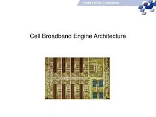

Cell Broadband Engine Architecture
E N D
Presentation Transcript
Idee und Entwicklung • Ursprüngliche Idee 1999: Ken Kutaragi ("Vater der PlayStation") • Kooperation von Sony, Toshiba und IBM • Alle drei in sehr unterschiedlichen Märkten aktiv • Mehr Absatz bedeutet niedrigere Preise • Erstes Ziel: Entertainment und Multimedia • Von Grund auf neu entwickelt
CPU Entwicklung The Need for Speed! • Wie wird Geschwindigkeit erreicht? • Taktrate (MHz) • Parallelität (CPI / IPC) • Speicher Bandbreite/Latenz (MB/s / ns) • Die Gegenspieler • Leistungsaufnahme (W) • Gate Delays (ns)
Techniken • Pipelining (Parallelität (CPI)) • Multithreading (gut gegen Speicherlatenz) • Superskalarität (noch mehr Parallelität) • Caches (noch besser gegen Speicherlatenz) • Höherer Takt (höhere Geschwindigkeit)
CPU Entwicklung • Heutzutage mehr Transistoren pro Chip möglich als nötig Beschleunigung von Spezialfällen durch Zusatzschaltungen • Out-Of-Order Execution für Instruktionen ohne Abhängigkeiten • Branch Prediction für innere Schleifen • SIMD für vektorisierbaren Code • Problem: Komplexe Schaltung führt zu höherer Leistungsaufnahme und geringerem Takt
Cell Design Ziele • Hohe Taktraten / Energieeffizienz • Sinnvoll? • Hoher Takt beschleunigt nicht nur Spezialfälle • Transistoren kommen langsam ins Schwitzen (Transistor Leakage) • „Auslagern“ von Schaltungen in Software (Compiler) muss nur einmal gemacht werden und kann von allen genutzt werden
Cell Design Ziele • Neues Design: Aus alten Fehlern lernen Keine bahnbrechenden Neuerungen in den Komponenten "I‘m certainly not inventing vector processors. One of the problems of being a pioneer is you always make mistakes and I never, neverwant to be a pioneer. It‘s always best to come second when you can look at the mistakes the pioneers made.“Seymour Cray
Cell Architektur Ziele erreicht?
Cell Specs Vergleichswerte • Intel & Co. Dualcore • 4 GHz P4? • P4: 12 GFLOPS • P4: 6,4 GByte/s • 235 Millionen Transistoren • 89 Watt • 1 Power Processing Element • 8 Synergistic Processor Elements • >4 GHz möglich • 256 GFLOPS (single precision) • 25,6 GByte/s Speicherbandbreite • 235 Millionen Transistoren • 60-80 Watt • 76 GB/s IO Bandbreite
Power Processor Element (PPE) • Betriebssystem / Verwaltung der SPUs • 64-Bit Power Architecture mit 2x32K L1 und 512K L2 Cache • PowerPC ISA, jedoch neue Mikroarchitektur Taktfrequenzvergleich mit G5 sinnlos
Mikroarchitektur • Dual-Issue Pipeline • Dual-Threaded • Altivec/VMX • Simple Branch Prediction • Keine OOO-Execution • 23-Stufen Pipeline Simple Architektur
RISC Eigenschaften • PPU / SPU ist RISC im ursprünglichem Sinne • Keine Kompatibilität zu älteren Architekturen notwendig • Hohe Taktraten durch simples Design • Orthogonaler Befehlssatz reicht einem Compiler Design an harten Grenzen orientiert
RISC Revisited • CISC: Viele Befehle teilweise interpretiert (Microcode) • RISC: Großteil der Befehle hart verdratet • Folge: Parallelität und Branch Prediction im Compiler umso wichtiger. • Aufgabe des Programmierers solange Compiler nicht verfügbar
Simple Branch Prediction • Branch Penalty: • Pipeline-Flush • Branch Target Berechnung • Instruction Fetch von der korrekten Adresse • 4k / 2Bit branch history table mit 6Bits global history per thread • Unnötige Branches sollten vermieden werden Branch Elimination
Branch Elimination if ( x < x1 ) { a = a0; } else if ( x < x2 ) { a = a1; } else if ( x < x3 ) { a = a2; } else if ( x < x4 ) { a = a3; } else { a = a4; } uint32_t x_lt_x1 = (uint32_t)((int32_t)(x - x1) >> 31); uint32_t x_lt_x2 = (uint32_t)((int32_t)(x - x2) >> 31); uint32_t x_lt_x3 = (uint32_t)((int32_t)(x - x3) >> 31); uint32_t x_lt_x4 = (uint32_t)((int32_t)(x - x4) >> 31); uint32_t result_0 = (x_lt_x4 & a3 ) | (~x_lt_x4 & a4); uint32_t result_1 = (x_lt_x3 & a2 ) | (~x_lt_x3 & result_0); uint32_t result_2 = (x_lt_x2 & a1 ) | (~x_lt_x2 & result_1); uint32_t result = (x_lt_x1 & a0 ) | (~x_lt_x1 & result_2);
Warum In-Order Execution? • OOO Schaltungen identifizieren Parallelität auf Instruktionsebene • Mit OOO und unveränderter Die-Größe würden ~2 SPEs wegfallen • Register Renaming typisch für OOO • Compiler können die Erkennung von Parallelität übernehmen Sehr komplexe Schaltung Zusätzlicher Schaltungsaufwand VLIW
Dual-Threading • Ähnlich Hyperthreading von Intel • Schnellerer Kontext Wechsel • Hilft Speicherlatenz zu verstecken • Hilft Execution Units besser auszulasten • Transistor Overhead von 5% beim P4 Energieeffizient
Microoperations • Im Beispiel: 1 Instruktion/Zyklus beim µOp-Decoder • 3 Instruktionen/Zyklus beim HW-Dekoder • µOps der PPE sind atomar und führen zum Pipelineflush! Programmierer sollte sie vermeiden
Microoperations • Multiple Load/Store • Automatisches Laden mehrerer Daten aus dem Speicher • Besser jedes Datum individuell zu laden • Bsp: lswi (Load String – 10 Zyklen Latenz) • Condition Register Recording Integer Instructions • Setzen von Flags im Condition Register nach einer Integer Operation • Assembleroperationen mit Punkt gekennzeichnet Vermeiden • Bsp: xor. (11 Zyklen Latenz)
Synergistic Processor Element (SPE) • Eigenständiger Prozessor • 128x128-Bit Register • Vector Processing • 256K Byte Local Store • DMA Controller / MMU • <5 Watt @ 4GHz
Registersatz der SPU • 128x128-Bit Register • Alle Operationen arbeiten auf Vektorregistern • Skalare Ergebnisse und Operanden im „Preferred Slot“
Beispiel Instruktionen • Floating Point Multiply Accumulate • fma $2,$3,$4,$5 R3: 18.0 20.0 5.0 10.0R4: 10.0 3.0 20.0 13.0R5: 20.6 60.3 50.9 15.2R2: 200.6 120.3 150.9 145.2
Beispiel Instruktionen • Rotate Word Immediate: • roti $2,$3,4 • R3:12345678 87654321 56781234 43218765R2:23456781 76543218 67812345 32187654
Beispiel Instruktionen • Rotate Quadword by Bytes Immediate: • rotqbyi $2,$3,4 • R3:0x00112233 0x44556677 0x8899AABB 0xCCDDEEFF R2:0x44556677 0x8899AABB 0xCCDDEEFF 0x00112233
Asymmetrische Pipelines • Dual-Issue 128Bit Pipeline • Even Pipe: Floating-Point + Fixed-Point Arithmetik • Odd Pipe: Bitmanipulation + Load/Store + Kontrolloperationen + Logische Operationen
Scheduling • Programmcode sollte die Asymmetrie beachten • Instruktionen an (2n)*Wortbreite even pipe • Instruktionen an (2n+1)*Wortbreite odd pipe
Local Store • 256K, 6 Zyklen, pipelined, single-ported SRAM • Enthält Instruktionen und Daten • SPU Adressraum spricht ausschließlich LS an • 128Byte/Zyklus Instruction Prefetch • 128Bit/Zyklus Daten • Kommunikation mit externen Komponenten durch DMA • 128 Bytes/Zyklus
Zugriff auf LS • PPE kann LS in den effektiven Adressraum abbilden Ermöglicht Zugriff von externen Komponenten Single-Ported Contention
Arbitrierung • Kombination aus Priorität und maximaler Belegungsdauer • SPE Inline Fetch (Instruction Fetch) niedrigste Priorität: • Instruction Fetch oft spekulativ • SPU Load/Store höhere Priorität: • Daten für Pipeline Ablauf benötigt
Memory Flow Controller (MFC) • Im Speziellen: DMA-Controller
DMA-Controller • Transfer von Daten: LS Hauptspeicher • Eigene MMU Austausch zwischen SPUs möglich • Transfergrößen: • 1, 2, 4, 8 Bytes • Vielfaches von 16 Bytes bis 16K (Alignment!) • DMA transferiert 128 Bytes pro Zyklus • Auch DMA Listen möglich Scatter/Gather • Transfer der Daten über den Element Interconnect Bus (EIB)
Element Interconnect Bus (EIB) • 4 Ringe mit je 128Bit Breite • 12 Hops • 96 Bytes/Zyklus Bandbreite 307,2 GB/s @ 3,2GHz Token Ring?
Kommunikation PPE / SPE • Über „Mailboxen“ • 32-Bit Register (In- / Outbound) • PPE: Ansteuerung über MMIO • SPE: Ansteuerung über Channel-Befehle • Geringe Latenz • Synchronisation
Fazit • Supercomputer-On-a-Chip • Musterbeispiel für Multicore • Energieeffizient • Designed für Multimedia • Komplexe Programmierung • Maximale Effizienz nur bei handoptimiertem Code
Praxistest Multigrid Finite Elemente Löser • 235 584 Tetraeder • 48 000 Knoten • 40 NKMG-Iterationen • In 5.8 Sekunden • Implementiert auf Simulator (Cell SDK) • Getestet auf Cell Blade @ 3,2 GHz Sustained Performance: 52 GFLOP/s