CCD based Vertex Detector for GLC
CCD based Vertex Detector for GLC. Yasuhiro Sugimoto KEK KEK/Niigata/Tohoku/Toyama Collaboration @VERTEX2003, Sep. 16, 2003. Outline. Project Overview of GLC Accelerator Detector CCD Vertex Detector Merit/Demerit of CCD at GLC/TESLA R&D Status

CCD based Vertex Detector for GLC
E N D
Presentation Transcript
CCD based Vertex Detector for GLC Yasuhiro Sugimoto KEK KEK/Niigata/Tohoku/Toyama Collaboration @VERTEX2003, Sep. 16, 2003 CCD based Vertex Detector for GLC
Outline • Project Overview of GLC • Accelerator • Detector • CCD Vertex Detector • Merit/Demerit of CCD at GLC/TESLA • R&D Status • Radiation Damage : Energy Dependence of Electron Damage • Dark Current, Flat-band Voltage Shift, Hot Pixels • Charge Transfer Inefficiency • Summary CCD based Vertex Detector for GLC
GLC Project • JLC has changed its name as GLC (Global Linear Collider) • 500GeV – 1TeV LC based on X-band linac • Future global organization is anticipated • Start experiment at 2013 CCD based Vertex Detector for GLC
GLC Accelerator CCD based Vertex Detector for GLC
GLC Acc. Parameters CCD based Vertex Detector for GLC
GLC Beam Structure GLC/NLC: Readout between trains ( 1 frame/6.7ms ) TESLA: Readout during trains ( 1 frame/50ms ) GLC/NLC is more favorable for vertex detectors CCD based Vertex Detector for GLC
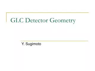
GLC Detector CCD based Vertex Detector for GLC
GLC Detector CCD based Vertex Detector for GLC
CCD Vertex Detector • Structure of CCD CCD based Vertex Detector for GLC
CCD Vertex Detector • Structure of CCD (Cont.) CCD based Vertex Detector for GLC
CCD Vertex Detector • Merits of CCD for Vertex Detectors • Very thin (~20mm) sensitive region (=Epitaxial (p-type) layer) Small multiple scattering • Diffusion of electrons in epitaxial layer • Key of excellent spatial resolution for CCD ( and CMOS ) • Takes time to diffuse : d = sqrt(Dt) ~ 6mm @ t=10ns OK for GLC/NLC (Fully depleted CCD at TESLA) • CCD has simple structure • Large area sensor • High yield CCD based Vertex Detector for GLC
CCD Vertex Detector • Demerits of CCD for Vertex Detectors • Long charge transfer path • Charge transfer inefficiency (CTI) by traps created by radiation damage • Long readout time Multi-port readout CP-CCD CCD based Vertex Detector for GLC
CCD Vertex Detector • Baseline Design of GLC Vertex Detector • R=24, 36, 48, 60 mm • |cosq| < 0.9 • s = 4 mm • Wafer thickness = 300 mm • B = 3T sb = 7 + 20/(pbsin3/2q) mm • This design is just a working assumption and the starting point of further R&D CCD based Vertex Detector for GLC
R&D Issues • Design Criteria : “The Highest Vertex Resolution with Technical Feasibility” • High spatial resolution of the sensors • Minimize multiple scattering Thin wafer • Close to the IP Radiation Hardness • Room temperature operation, if possible Next milestone: sb = 5 + 10/(pbsin3/2q) mm CCD based Vertex Detector for GLC
R&D Status • Spatial Resolution: • < 3mm has been demonstrated by beam tests • Thin Wafer: • Partially thinned (honeycomb type) wafer is being designed ( average thickness ~ 100 mm ) • Radiation Damage Study: • Neutron damage study by Cf-252 • Electron damage study by Sr-90/150MeV beam CCD based Vertex Detector for GLC
Electron Damage Study • Damage in CCDs • Surface Damage • dE/dx in SiO2 • Surface dark current • Flat-band voltage shift • Bulk Damage • Lattice dislocation in Si bulk • Bulk dark current • Charge transfer inefficiency (CTI) Trap Levels CCD based Vertex Detector for GLC
Electron Damage Study • Expected Beam Background at GLC • At LC, e+/e- pair background is created at IP through beam-beam interaction • Simulation using generator ‘CAIN’ and GEANT4-based simulator ‘JUPITER’ CCD based Vertex Detector for GLC
Electron Damage Study • Test Sample CCDs • 256x256 pixcels • Made by Hamamatsu • Readout Freq : 250kHz • Readout Cycle : 2 sec • Irradiation: • At room temperature • Without bias/clock • Sr-90: 0.6, 1.0, 2.0 x 10¹¹/cm2 • 150 MeV beam: 0.5, 1.0 x 10¹¹/cm2 CCD based Vertex Detector for GLC
Electron Damage Study • NIEL Hypothesis • Bulk damage is thought to be proportional to non-ionizing energy loss (NIEL) • NIEL of electrons has strong energy dependence • e+/e- pair background hitting the inner-most layer of VTX at LC peaks at ~20MeV High energy electron beam irradiation test Sr-90 GLC b.g. CCD based Vertex Detector for GLC
Electron Damage Study • Dark Current • Surface dark current is very well suppressed by using MPP (multi pinned phase) mode (inverted mode) • In MPP mode, dark current is dominated by bulk current CCD based Vertex Detector for GLC
Electron Damage Study • Dark Current (Cont.) CCD based Vertex Detector for GLC
Electron Damage Study • Flatband Voltage Shift • Surface damage in SiO2 (positive charge build-up) causes shift of operation voltage • FVS is observed as shift of MPP threshold • No significant FVS is observed up to 2x10¹¹e/cm2 irradiation Amplitude of Negative Clock Voltage (V) CCD based Vertex Detector for GLC
Electron Damage Study • Dark Current Pedestal • In MPP mode, however, spurious dark current (dark current pedestal: DCP) which is generated during clocking is observed • This DCP is thought to be due to impact ionization by holes trapped in Si-SiO2 interface levels CCD based Vertex Detector for GLC
Hot Pixels Measured at +10 C Cycle Time: 2 sec Electron Damage Study • 150MeV Beam • Before Irradiation • 0.5x10¹¹/cm2 • 150MeV Beam • Before Irradiation • 1x10¹¹/cm2 • Sr-90 • 1x10¹¹/cm2 • 2x10¹¹/cm2 CCD based Vertex Detector for GLC
Electron Damage Study • Hot pixels • Average dark current of 150MeV beam irradiated CCD is x2~5 larger than Sr-90 irradiated CCD • But hot pixel generation rate is completely different • This could be due to cluster-defect generation by high-energy electrons CCD based Vertex Detector for GLC
Electron Damage Study • Charge Transfer Inefficiency (CTI) • Derived from position dependence of Fe-55 X-ray(5.9keV) peak • CTI induced by 150MeV beam is x2~3 larger than Sr-90 induced CTI Beam Sr-90 CCD based Vertex Detector for GLC
Electron Damage Study • CTI Improvements • Notch Channel: • Narrower channel with additional implant • Charge packets encounter less traps CCD based Vertex Detector for GLC
Electron Damage Study • CTI Improvements (Cont.) • Fat-zero Charge Injection: Fill-up traps with artificially injected charge ~1200e Fat-zero Injection with LED CCD based Vertex Detector for GLC
Electron Damage Study • CTI Improvements (Cont.) • Wider Vertical Gate Clock & Faster Horizontal Clock CCD based Vertex Detector for GLC
Electron Damage Study • CTI Improvements (Cont.) • Reduction of number of transfer ( Increase number of output port) Multi Thread CCD (MT-CCD) • Expected CTI • Notch channel, f=20MHz, tw=40ms, fat-zero=500e • VCTI=2x10⁻⁵, HCTI=4x10⁻⁶ / 1x10¹¹e/cm2 @27C • 32(V)x2000(H) pixels 0.06%(V), 0.8%(H) signal loss • R=24mm, B=3T ~20% signal loss after 50 years • R=15mm, B=4T ~25% signal loss after 20 years CCD based Vertex Detector for GLC
Summary • We are studying CCD-based vertex detector for GLC(/NLC) which has beam structure favorable for CCD (or any other) vertex detector • In order to estimate radiation damage effect by e+/e- pair background at LC, electron damage effects on CCDs are studied for both Sr-90 b and 150MeV beam irradiated CCDs. We found : • 150MeV electrons cause • x2 ~ x5 larger bulk dark current than Sr-90 • x2 ~ x3 larger CTI • larger dark current pedestal at higher temperature • hot pixels, which cannot be found in Sr-90 irradiated CCD • no significant flat-band voltage shift up to 2x10¹¹e/cm2 irradiation • CTI suppression by notch channel and fat-zero injection CCD based Vertex Detector for GLC
Summary (cont.) • Using a model calculation, CTI suppression by wider vertical clock and faster horizontal clock has been shown. • Combining all the CTI improve methods, and comparing with background simulation, we expect life of CCD-based vertex detector is • ~50 years with R=24mm, B=3T (baseline design) • ~20 years with R=15mm, B=4T even at room temperature. If CCD is cooled ( < -70 C ), CTI becomes still better. Dark current pedestal or hot pixels could put possible limitation for room temperature operation, rather than CTI • If the design with R=15mm is possible, and thinner (~100mm) wafer is used, impact parameter resolution is improved from sb = 7 + 20/(pbsin3/2q) mm (baseline design) tosb = 5 + 10/(pbsin3/2q) mm, which is the milestone of our R&D. CCD based Vertex Detector for GLC