Download
1 / 9
110 likes | 379 Vues
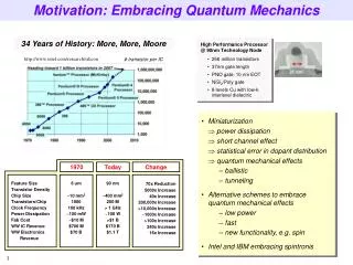
Motivation: Embracing Quantum Mechanics. http://www.intel.com/research/silicon. # transistor per IC. 34 Years of History: More, More, Moore . High Performance Processor @ 90nm Technology Node • 256 million transistors • 37nm gate length • PNO gate: 10 nm EOT • NiSi 2 /Poly gate

E N D
Motivation: Embracing Quantum Mechanics http://www.intel.com/research/silicon # transistor per IC 34 Years of History: More, More, Moore High Performance Processor @ 90nm Technology Node • 256 million transistors • 37nm gate length • PNO gate: 10 nm EOT • NiSi2/Poly gate • 8 levels Cu with low-k interlevel dielectric • Miniaturization • power dissipation • short channel effect • statistical error in dopant distribution • quantum mechanical effects • – ballistic • – tunneling • Alternative schemes to embrace quantum mechanical effects • – low power • – fast • – new functionality, e.g. spin • Intel and IBM embracing spintronis 1970 Today Change Feature Size Transistor Density Chip Size Transistors/Chip Clock Frequency Power Dissipation Fab Cost WW IC Revenue WW Electronics Revenue 6 um ~10 mm2 1000 100 kHz ~100 mW ~$10 M $700 M $70 B 90 nm ~400 mm2 200 M > 1 GHz ~100 W >$1 B $170 B $1.1 T 70x Reduction 5000x Increase 40x Increase 200,000x Increase >10,000x Increase ~1000x Increase >100x Increase 240x Increase 16x Increase
Successful Examples of Spintronics metal-based ferromagnetic devices GMR spin valve hard drive read head magnetic tunneling junction memory • Rapid transition from discovery to commercialization • – 1988 giant magneto resistance (GMR) • – 1998 IBM read head extends storage from 1 to 20Gbits ($100B) • – 2004 Motorola MRAM with 10ns access time • – 2010 10Gbit memory chip projected • Non-volatile, no wearout, fast write time, fast read time, low energy for writing, radiation-hard www.sematech.org/meetings/ past/20021028/17_Hummel_Mram.pdf
Objective spin ballistic length 100nm • All existing semiconductor devices operate in the diffusive transport regime, where scattering results in heat dissipation and limits frequency response • Spin transport in the ballistic regime offers opportunities which are heretofore unexplored and unexploited • Demonstrate the essential elements required for • ballistic spin devices – semiconductor spin-FET • Essential elements: • electrical (rather than optical) • injection of highly spin-polarized electrons • manipulation of electron spin orientation during coherent transport • spin-sensitive detection InAs spin transistor
Semiconductor spintronics: Spin FET Datta and Das, Applied Physics Letters, 56, 665 (1990); 816 citations • Ferromagnetic source injects spin polarized electrons • Gate controlled spin precession through Rashba spin-orbit coupling in 2D channel • Ferromagnetic drain that provides: • low resistance if spins are parallel • high resistance if spins are anti-parallel • Not experimentally demonstrated yet • Key processes face challenges
Our Technical Approach: Electrical + InAs • Key obstacle • to study spin manipulation in InAs, ferromagnetic/InAs needed • to develop FM/InAs hybrid junction, spin detection needed • optical detection is not practical, electrical detection needed • FM/InAs hybrid junction needed for electrical detection Our solution: a novel configuration for electrical spin injection and detection Manipulation Injection Efficiency of spin transport across FM/InAsjunction Electrical tunability of Rashba SO coupling in InAs Detection Electrical spin detection • Challenges • determination of R • control of R • optimization of R • Challenges • optimal ferromagnetic • Interface integrity • etching selectivity
Current Status: Ferromagnetic/GaAs Hybrid Junction 5 meV Fe GaAs Metal oxide Al2O3 40% Al2O3 Tunneling PQW to 40% (lower bound, 5 K) Fe GaAs Magnetic Metal / Tunnel Barriers (NRL) 32% Schottky PQW • Benchmark performance at 5K • well-defined system state • detector “purely” excitonic • most well studied temperature Fe AlGaAs GaAs APL 80, 1240 (2002) (NRL) APL 82, 4092 (2003) (NRL)
Past Spin Research : Optical + GaAs Pcirc PQW • GaAs band gap is ideal for optical experiments • optically generate spin-polarized electrons • detect spin populations with circularly polarized PL Pump-Probe Studies of Spin Precession Spin-Light Emitted Diode Fe/barrier/GaAs NRL patent (1999) D. D. Awschalom, UCSB
Rashba Spin-Orbit Coupling z z 2DEG in quantum well confinement potential rest frame moving frame relativistic effect Bin Structural Inversion Asymmetry • In nature, spins are controlled with magnetic field. • Thanks to spin-orbit coupling, now spins can also be controlled by using conventional gates. Bin In the absence of an external B
Optimal Material for Rashba Spin-Orbit Coupling InAs 2ħwSO (meV) Si GaAs BIN (Tesla) • Advantage of InAs • Larger g* (15 vs. 2 vs. 0.44) Larger spin splitting (meV) • Smaller m* (0.023 vs. 0.067 vs. 0.19) Larger quantization energy (10meV) • Higher RT mobility (40k vs. 8k vs. 1.4k) Longer mean free path (700nm)