Download

1 / 15
160 likes | 463 Vues
Welcome to Wootton Bassett! Wave Solder Process – Back To Basics. Nigel Burtt Production Engineering Manager Dolby Laboratories, Inc. – European HQ. Lead-Free Wave and Selective Soldering Workshop. Wave solder process timeline (single-wave). Solder solidified and joint formed.

E N D
Welcome to Wootton Bassett!Wave Solder Process – Back To Basics Nigel Burtt Production Engineering Manager Dolby Laboratories, Inc. – European HQ Lead-Free Wave and Selective Soldering Workshop SMART Group Lead-Free Wave & Selective Soldering Workshop Dec 5th 2007
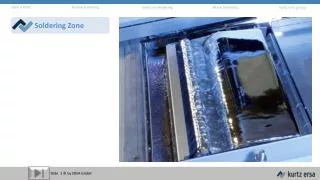
Wave solder process timeline (single-wave) Solder solidified and joint formed Flux activated, solvent evaporated, thermal shock minimised Solder wetting complete Wave solder process wetting time Dwell time Flux Applied Soldering Preheat Cooling Solder drainage complete Complete coverage of PCB and penetration of PTHs Solder contact made Solder contact lost SMART Group Lead-Free Wave & Selective Soldering Workshop Dec 5th 2007
Lead-Free No-Clean Wave Solder Process Setup –Five Priorities • DWELL TIME • CONVEYOR SPEED • PREHEAT • FLUX APPLICATION • SOLDER TEMPERATURE All these parameters need to be in balance - some compromises will be required SMART Group Lead-Free Wave & Selective Soldering Workshop Dec 5th 2007
Lead-Free No-Clean Wave Solder Process Setup –First Priority = Dwell Time • Set dwell time in solder wave to be within about 2-4 seconds • Solder wave flow both forwards and backwards over the nozzle as the PCB comes into contact • Solder flow velocity should be roughly equal to the conveyor speed • Dross and flux residue move away from the PCB SMART Group Lead-Free Wave & Selective Soldering Workshop Dec 5th 2007
Dwell Time • Solder wave height and conveyor speed control the dwell time • Approximately a 2-4cm solder contact window is desirable as the PCB passes over the wave. • Rough rule of thumb Dwell time (secs) contact window (cm) / conveyor speed (m/min) • The wave surface should be exactly parallel to the PCB contact window, contact timing across the wave should be coincident within 0.2 seconds • Physical adjustment of the machine level, nozzle level and conveyor heights may be necessary to achieve the correct parameter balance. • Conveyor should present PCB to wave at an angle of around 70 Parallel to wave 20-40mm 70 SMART Group Lead-Free Wave & Selective Soldering Workshop Dec 5th 2007
Dwell Time must be optimised for each PCB design From www.wavesoldering.com SMART Group Lead-Free Wave & Selective Soldering Workshop Dec 5th 2007
The Importance of Parallelism From www.wavesoldering.com SMART Group Lead-Free Wave & Selective Soldering Workshop Dec 5th 2007
Lead-Free No-Clean Wave Solder Process Setup –Second Priority = Conveyor Speed • Set conveyor speed to between 0.7-1.5m/min • Setting must be carefully balanced against dwell time and preheat requirements for each PCB design • Faster = less dwell time, less preheat • Slower = more dwell time, increased preheat SMART Group Lead-Free Wave & Selective Soldering Workshop Dec 5th 2007
Lead-Free No-Clean Wave Solder Process Setup –Third Priority = Preheat • Set preheaters to provide a topside temperature on the PCB of around 90-1300C immediately before solder contact • Utilise the different types of preheat available to provide an even ramp rate • Setting must be balanced against solder dwell time • Preheat requirement depends on flux type and carrier solvent • Also dependent on PCB thickness and/or fixture thermal mass • PCB underside should not exceed 1500C before the wave • Purpose is to activate the flux and allow it time to work • Also brings the PCB and components up to a suitable working temperature to minimise thermal shock during solder contact and to promote wetting during soldering • Important that the preheat drives off the flux base solvent, to prevent solder spitting during wave contact. • Especially for VOC-free (water-based) no-clean fluxes SMART Group Lead-Free Wave & Selective Soldering Workshop Dec 5th 2007
Lead-Free No-Clean Wave Solder Process Setup –Fourth Priority = Fluxer • Set fluxer to give complete and uniform coverage of PCB to be soldered and full penetration of all plated-through holes • Recommended application rate is approx 75ml/cm2, but depends on flux type and solvent carrier. • Too little flux will result in bridging and other such defects • Too much will lead to increased residue and solder balling • Use old thermal transfer fax paper in a fixture to check on flux coverage From www.ecd.com SMART Group Lead-Free Wave & Selective Soldering Workshop Dec 5th 2007
Lead-Free No-Clean Wave Solder Process Setup –Fifth Priority = Solder Temperature • Set the solder pot temperature to suit your lead-free alloy • For SnAg3.8Cu0.7, the melting point is 2170C, but the pot will have to run with superheat above this temperature to optimise the flow characteristics of the alloy • If run too hot, the topside temperature on the PCB during wave contact may affect SMT solder joints, even causing secondary reflow in extreme cases. • Don’t rely upon the machine thermocouple to set, use a separate thermocouple directly in the wave to check the solder contact temperature accurately. • Typically the running wave should measure around 2600C SMART Group Lead-Free Wave & Selective Soldering Workshop Dec 5th 2007
Measurement Tools From www.rswww.com From www.solderstar.com From www.intertronics.co.uk SMART Group Lead-Free Wave & Selective Soldering Workshop Dec 5th 2007
Example of Dolby Process SMART Group Lead-Free Wave & Selective Soldering Workshop Dec 5th 2007
Wetting Test PCB as final check SMART Group Lead-Free Wave & Selective Soldering Workshop Dec 5th 2007
Any Questions? SMART Group Technical Committee info@smartgroup.org +44(0) 1494 465217 Nigel Burtt - Production Engineering Manager Dolby Laboratories, Inc. - European HQ njb@dolby.co.uk +44(0) 1793 842132 (c) SMART Group 2007 We accept no liability for the consequence of any action taken on the basis of information provided from us. The information is provided in good faith. Any views or opinions presented to you are solely those of the author and reflect their understanding of current good practice and their interpretation of guidance, regulation and standards. SMART Group Lead-Free Wave & Selective Soldering Workshop Dec 5th 2007