Clock Synchronizers Project Progress Presentation D0827
Explore various solutions to synchronization problem of Plesiochronous, Periodic, and Asynchronous classes, their design, testing, and results.


Clock Synchronizers Project Progress Presentation D0827
E N D
Presentation Transcript
SoC Clock Synchronizers Project Progress Presentation D0827 Students: Elihai Maicas Harel Mechlovich Instructor: Shlomi Beer-Gingold
Presentation Agenda • Abstract • Introduction • Hardware • Software • Conclusions • Appendix
Abstract • Project essence • The synchronization problem becomes more and more common • The project's main objective is to examine several solutions to the synchronization problem of classes Plesiochronous, Periodic and Asynchronous • General working mode • The verious synchronizers were designed and programmed to an FPGA device
Abstract cont. • A test circuit was designed to envalope the different DUTs in order to test them for correctness and performance • General requirements • The project’s main objective was to test the different solutoins for: • Correctness • Several parameters such as: latency, area, power, simplicity and plug & play capabilities
Abstract cont. • Results • All synchronizers were tested and were proven to be working or not • The different parameters were calculated for the verious solutions • We’ve made some conclusions including recomandations regarding when to use each of the synchronizers
Introduction • The project covered 5 selected synchronizers • The synchronizers match 3 different synchronization classes: • Plesiochronous • FIFO Synchronizer with Multisynchronous Support • Two-Register Synchronizer with Conflict Detector • Periodic • Two-Register Synchronizer with Conflict Detector and Predictor • Asynchronous • Two-Flop (AKA Brute-Force) Synchronizer • General Purpose Asynchronous FIFO Synchronizer
Introduction cont. • FIFO Synchronizer with Multisynchronous Support Plesiochronous
Introduction cont. • Latency • . • Does not include null injections • Pros • No chance of synchronization failure • Cons • Quite a long latency • Requires design consideration – not a plug & play device Plesiochronous
Introduction cont. • Two-Register Synchronizer with Conflict Detector Plesiochronous
Introduction cont. • Latency • . • Pros • Delay components required only for clocks • Plug & Play • Cons • Small, but not zero, chance of sync failure • Area Plesiochronous
Two-Register Synchronizer with Conflict Detector and Clock Predictor Introduction cont. Periodic
Introduction cont. • Latency • . • Pros • Delay components required only for clocks • Plug & Play • Cons • Small, but not zero, chance of sync failure • Area Periodic
Introduction cont. • Two-Flop (AKA Brute-Force) Synchronizer Asynchronous
Introduction cont. • Latency • . • Pros • Easy to implement • Cons • Latency! Asynchronous
Introduction cont. • General Purpose Asynchronous FIFO Synchronizer Asynchronous
Introduction cont. • Latency • No actual synchronization delay • Pros • No delay • No failures • Cons • Extremely expansive in area • Not a plug & play device
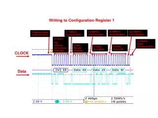
Introduction cont. • The board • Was programmed with the different synchronizers and a general test circuit that operates the DUTs and examines them in terms of correctness and latency • Interface is done using a DLP device used for writing to internal config registers
Introduction cont. • Operation • Board • DLP • PC • GUI • Results + + +
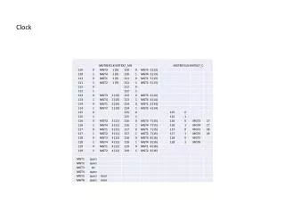
Hardware • Block level • addr_pntr • Ctrl (Registers) • latency_chk • Sync • DRAM_SRC & DRAM_DST • comperator • mis_cntr
Hardware cont. • DLP voltage connectivity • All control and data bits were shorted to relevant signals in the design through the J5 wide connector on the XUP board
Hardware cont. • DLP FSM • The satate machinecommunicates with thedesign according to theDLP protocol
Software • Used applications • RTL Simulations: ModelSim • Synthesis: Symplify Pro • P&R: Xilinx ISE • RTL coding • VHDL
Summary & Conclusions • Results • Out of 5 synchronizers tested all 5 were found to be working • Latency, power and area were measured for working synchronizers • Sampled latency was stored in 18 bins with a range of 5ns each • Power was determined by current measurement on board • Area was pulled out of synthesis results
Summary & Conclusions cont. • Plesio FIFO Synchronizer • Expected Av. latency of ~62.5ns • Area • LUT2: 2 • LUT3: 3 • LUT4: 6 • FDC: 58
Summary & Conclusions cont. • Plesio Synchronizer with conflict detector • Expected Av. latency of ~12.5ns • Area • LUT2: 3 • LUT3: 34 • LUT4: 4 • FDC: 39 • MUXF: 15
Summary & Conclusions cont. • Periodic Synchronizer with conflict detector • Expected Av. latency of ~15ns • Area • LUT2: 3 • LUT3: 31 • LUT4: 4 • FDC: 67 • MUXF: 16
Summary & Conclusions cont. • Async Synchronizer • No latency • Area • LUT: 40 • FF: 40 • Block RAM: 1
Summary & Conclusions cont. • Brute-force Synchronizer • Latency of 60ns • Area • LUT2: 2
Our Legacy • DLP module • Configure design registers • Standart MAS format • Macro tull bar • RTL modules • Plug & Play • General