The Memory System: Memory Hierarchy
The Memory System: Memory Hierarchy. A Memory System is normally comprised of a hierarchy of memories: Cache - very fast (1 or 2 cycle access), but small (e.g. 32 KB-64 KB) built with SRAM on-board the processor chip

The Memory System: Memory Hierarchy
E N D
Presentation Transcript
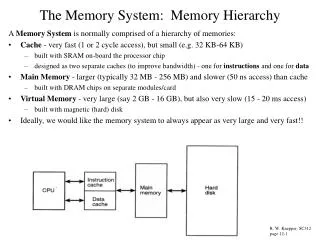
The Memory System: Memory Hierarchy A Memory System is normally comprised of a hierarchy of memories: • Cache - very fast (1 or 2 cycle access), but small (e.g. 32 KB-64 KB) • built with SRAM on-board the processor chip • designed as two separate caches (to improve bandwidth) - one for instructions and one for data • Main Memory - larger (typically 32 MB - 256 MB) and slower (50 ns access) than cache • built with DRAM chips on separate modules/card • Virtual Memory - very large (say 2 GB - 16 GB), but also very slow (15 - 20 ms access) • built with magnetic (hard) disk • Ideally, we would like the memory system to always appear as very large and very fast!! R. W. Knepper, SC312 page 12-1
Memory Systems: Hierarchy • Concept of an infinite cache: • fetches by the CPU for instructions or data normally come from cache (say 95% of time) • if instructions or operands are not in cache, a "miss" occurs and CPU waits while MMU (memory management unit) goes to main memory for the missing instruction or operand • on the very rare occasion that the operand or instruction is not in main memory, the CPU must go to the hard disk to find it (while the processor either waits idle or branches) • most of the time the instructions/data are available in cache giving the appearance of a large, fast memory! • Memory addressing: 32 bit address can access 4 GB of data/instructions • Speed & Cost of 4GB DRAM Main Memory: • if all memory were only main memory (DRAM), 4 GB would cost $24,000 at $6/MB • access time would be only 50 ns, rather than the 2-3 ns obtainable with on-board cache • Memory hierarchy is essential to achieving high speed, large memory, & low cost!!! R. W. Knepper, SC312 page 12-2
The Ideal Memory System • Memory hierarchy "synergy": Can we have our cake and eat it too? • Assume the memory hierarchy on the previous chart is comprised of the following: • 2 on-chip 32 MB caches running at 3 ns cycle time (single cycle cache) • perform instruction fetch from I-cache while concurrently fetching operands or writing data in D-cache • assume we find instructions and data in the caches (hit) 95% of the time • 64 MB DRAM main memory operating at 50 ns cycle time • assume of the 5% cache misses, we find the data in main memory 99.9999% of the time, i.e. we have to go to the hard disk drive for the data or instructions only 0.000005% of the time • 4 GB hard disk (virtual memory) with a 16 ms latency (random access time) • Apparent access time: • (0.95 x 3 ns) + (0.04999995 x 50 ns) + (5E-8 x 16 ms) = 6.15 ns • System cost: • SRAM cache adds ~$70 to cost of processor chip • DRAM cost = ~$380 at $6/MB • 4 GB Hard disk cost = ~$200 • Total cost to system = ~$650 • By all appearances, we have achieved our goal of a very large, very fast, and very cheap memory system! R. W. Knepper, SC312 page 12-3
Why it works: Locality of Reference • temporal locality • programs tend to contain loops (often nested loops) where an instruction and/or data are accessed many times in sequence • spacial locality • instructions and/or data that are stored in contiguous (neighboring) locations are often repeatedly accessed for reading or writing in a typical program • memory heirarchy makes use of temporal and spacial locality by transferring at one time a group of instructions/data into cache or into main memory • A group of instructions or data transferred from main memory into cache is called a line of data (say 32 bytes) • A group of instructions or data transferred from disk storage into main memory is called a page of data (say 4K bytes) • Virtual memory = the appearance that all 4GB addressable memory resides in main memory • Studies of the execution of computer programs have demonstrated the importance of locality of reference in designing a hierarchical memory system. • Temporal and spacial locality allow us to achieve a near infinite cache in practice for the operation of most computer programs! • thrashing = phenomenon of frequent disk accesses due to a particular program perhaps accessing a database which does not fit entirely into main memory • Solution: need a larger main memory! R. W. Knepper, SC312 page 12-4
Cache Memory Organization • Cache organization schemes: • direct mapped • fully associative • set-associative • Line: A block of data transferred into cache at a given time (4B in text illustrations) • the memory address is comprised of 5 bit tag, 3 bit index, and 2 bit byte fields • the cache stores both the data (line) as well as the main memory address (tag) of the data • Hit and Miss • When CPU requests data from cache, the address of requested data is compared with addresses of data in cache. If both tag and index addresses match (called a cachehit), the requested data is present in cache • data word (or byte) is transferred to CPU • If the address of requested data does not match tag plus index address of data present in cache, the cache signals the CPU that a cachemiss has occurred. • Main memory transfers a new line (containing the requested data word) into the cache and also sends the requested word (or byte) along to the CPU • When a cache miss occurs and a new line of data is to be transferred in from main memory, the cache is likely already full of existing data lines so that one of them needs to be replaced with the new data line. If the line to be replaced has been changed since it was brought in from main memory, it must be written back into main memory first. R. W. Knepper, SC312 page 12-5
Direct Mapped Cache • cache address given by the index address bits • Example at left: 8 lines stored in cache with 3 index address bits • a memory line can be mapped to only one location in cache given by the index address • on a cache access, tag bits for given index are compared with the CPU address tag bits • cache hit: tag bits are identical to address tag • word is fetched from cache and sent on the bus to the CPU • cache miss: tag bits do not match address tag bits • cache sends signal to main memory to fetch the correct line with matching tag address bits • new line of data (or instructions) is sent both to the CPU and to update the cache • direct mapping is not usually the most optimum for improving cache hit ratio due to allowing only one index address in cache at any one time R. W. Knepper, SC312 page 12-6
Fully Associative Cache Mapping • Any memory line can be placed into any location in the cache • no limitation to only store one line of data for a given index address as in the direct mapped cache • Tag address now includes the three bits that were previously labeled index address • When a request for data comes from the CPU, the entire main memory tag address must be compared with all tag addresses presently residing in the cache (next chart), to see if the requested data word is in the cache. • If not, a miss occurs and a new data line (with the requested word) is brought into the cache from main memory R. W. Knepper, SC312 page 12-7
Associative Memory for Tag Address Compare • Associative memory technique is used in cache SRAM chip to compare requested Tag address bits with those of lines currently residing in the cache • Tag address field (4 bits shown) is used to carry out an associative search during access • a compare of the tag address bits with all tags stored in cache is done in parallel • match logic (comprised of XOR’s and a NOR) is implemented at each row line for tag address array portion of cache • M=1 indicates a match for that particular Tag • if a match occurs for any cache word, a cache hit is indicated on Hit/miss’ output and that particular word line is selected in the cache • if no match occurs for any of the tag addresses stored in cache, the Hit/miss’ output is zero and signals main memory that a cache miss has occurred • high circuit cost for a fully associative cache R. W. Knepper, SC312 page 12-8
Two-way Set Associative Cache Mapping • A set associative cache is a compromise between direct mapped and fully associative cache approaches • Index bits again specify cache (set) address • can have two lines of data per set (2-way set associative) with two different tag addresses or four lines of data per set (4-way set associative) with four different tag addresses • Example at left: 2 index bits 4 sets with two-way set associative organization • more realistic example: 16KB cache with 4-way set associativity, 16 bit address • line size = 16 words = 64 bytes 256 lines in the cache • 4 groups of 64 sets of 64B lines in the cache 6 bits in index address, 6 bits for word & byte fields • with a 16 bit address, there would be 4 bits left for the tag address R. W. Knepper, SC312 page 12-9
Set-Associative Cache Block Diagram • Cache must have logic to perform 2-way or 4-way compare of cache tag bits with CPU address tag bits • if tag bits in cache match the CPU tag address, one of the match logic outputs is “1” • the selected word is gated out to the CPU/Main Memory bus by the tri-state buffer • only one match can occur for a given tag address • a logic OR gate pulls Hit/Miss’ line high to signal to CPU a Hit is achieved • If the Tag address from CPU does not match any stored Tags, then both Match logic circuits give zero outputs, pulling the Hit/Miss’ line low to signal the CPU and main memory that a cache Miss has occurred. R. W. Knepper SC312 page 12-10
Set-Associative Cache with 4-word Lines • Cache lines are normally defined to contain many words • 2n where n is the number of bits in the Word address field • (earlier examples had assumed only one word per line for simplicity of the charts) • Example below: • a Line contains 4 Words (each Word has 4 Bytes) implying 2 address bits in the Word field • the Index address contains 2 bits implying 4 sets of lines specified by the Index address • 10 bit address implies 4 bits in the Tag address field • 2-way set associative organization implies that a given line of data can be in either the “left” or “right” side of the cache at the specified location given by index address bits R. W. Knepper, SC312 page 12-11
Cache Write/Replacement Method Cache Replacement Algorithm: • In the event of a cache miss, assuming all lines are filled in the cache, some existing line must be replaced by the new line brought in from main memory! Which line to replace? • random replacement scheme • FIFO scheme • LRU (least recently used) algorithm • a crude approximation to the LRU approach is often used • Line size: bus between CPU and cache and between cache and memory is made as wide as possible, based on the line size • line size is a tradeoff between bandwidth to cache vs cost and performance limitations • Cache Write Methods: • Write-Through • the result is written to main memory (and to the cache if there is a cache hit) • write buffering sometimes used to avoid a slow down • Write-Back (also called copy-back) • CPU write only to the cache (assuming a cache hit) • if a cache miss occurs, two choices are possible • write-allocate: read the line to be written from main memory and then write to both main memory & cache • write back only to main memory • Valid bit: indicates that the associated cache line is valid • Dirty bit: indicates that a line has been written in cache (dirty in main memory) R. W. Knepper, SC312 page 12-12
256K Cache Example – Block Diagram • 256KB memory with 2-way set associativity and write-through approach • 32 bit memory address with byte addressing capability • line size = 16 bytes = 4 words 2 bits each for word address and byte address • index field = 13 bits 8192 sets • tag field = 15 bits • 2-way set associativity 16,384 line entries in cache = 64K words = 256K bytes R. W. Knepper SC312 page 12-13
256K Cache Block Diagram Description (continued) • each cache entry contains 16 bytes of data (line) + 15 bit tag address + 1 valid bit • 4-to-1 selector chooses desired word from addressed line based on 2 word address bits • 2 tri-state buffers drive CPU data bus depending on which Tag memory has valid match • AND gate requires match logic "1" plus valid bit "1" plus Read line high to enable buffer • data bus between cache and main memory is 128 bits wide • entire line transferred at once • Main memory address bus and CPU data bus are both 32 bits wide • 32b CPU data bus fanned-out to 128b memory data bus for write to memory • 1 word only is selected based on word address • 4-to-1 MUX plus buffer (driver) provide load from memory to CPU on a cache miss • Hit/miss line signals both CPU and main memory on a cache miss or cache hit • Cache control logic determines if operation is a read or write to cache • if a write, cache control determines in which of the two tag locations to write the word R. W. Knepper SC312 page 12-14
256K Cache Example – Read and Write Operations • Cache access at address = 0F3F4024h (0000 1111 0011 1111 0100 0000 0010 0100) • Tag = 079Fh (000 0111 1001 1111), Index = 1402h (1 0100 0000 0010), Word = 01 • Read Operation assuming a Hit Occurs: • Index address bits 1402h selects row in cache and compares Tag bits with CPU Tag address • Word address bits 01 select specified Word in both Data Memory 0 and 1 • Match logic shows match between tag bits of CPU address and cache tag entry (say Memory 0) • If also valid bit is “1” and Read is “1”, then tri-state 0 gates out selected Word to CPU data bus • Hit/Miss’ line signals a Hit has occurred to CPU and Main Memory • Read Operation assuming a Miss Occurs: • Index and Word addresses set up as above, but Match logic circuits show no match • Hit/Miss’ line is low signaling to CPU and Memory that a Miss has occurred • Cache Control specifies which line to replace with a full 128b new line from Main Memory • 4-to-1 MUX selects requested 32-bit Word from 128-bit Line to send on to the CPU • Write Operation assuming a Hit Occurs: • CPU address selects Index (row) and Word in which to write • 32-bit Word is fanned-out to each of the four words on 128-bit memory data bus • If Hit occurs with Tag address, 32-bit word is written to specified location • Write Operation assuming a Miss Occurs: • Hit/Miss’ line signals a Miss; Word is written to Main Memory (or to both in Write-Back case) R. W. Knepper, SC312, page 12-15
Additional Cache Hierarchy Design Issues • Instruction and Data L1 Caches: • two separate caches for instructions and for data increases bandwidth from CPU to memory • fetch instructions while at same time write or fetch data • two separate caches allows individual (simpler) design • instruction cache may be direct mapping while data cache may be 2-way or 4-way set associative • sometimes a single cache (unified cache) is more economical/practical • Multiple-Level Caches: • a second level of cache (L2) often improves "infinite cache" access time • if L1 cache miss occurs, we go to L2 for instructions/data • L2 access time (latency) may be only 2X-4X longer than L1 cache • improvement over main memory which may be 10X-20X longer latency • allows use of smaller single cycle L1 cache and larger 3-4 cycle L2 cache nearby • L2 may be on a separate chip on the back side of module, or due to recent VLSI advances with 0.18 um and 0.13 um litho capability, it may be on the same chip • example: Intel Coppermine Pentium III • example: AMD Athlon processor • example: recent IBM Power4 PPC processor has 1.5 MB of shared L2 cache on chip with 2 processors each having their own L1 caches R. W. Knepper, SC312 page 12-16
Virtual Memory Concept and Implementation • Virtual Memory is large memory storage addressable by 32 bit (or higher) memory address but beyond the size capability of the physical address space in main memory • desire that virtual memory appears to the CPU to be main memory • addressability • average latency not to exceed main memory access time by very much • each program sees a memory space equal to the virtual address space • the hardware must map each virtual address into a physical address in main memory • Virtual address space from different programs may map to the same physical address space • Allows code and data to be shared across multiple programs • normally implemented with hard disk (or tape drive) storage • Pages: Blocks of addresses in virtual memory which map into physical page frames of identical size in main memory • analogous to "line" in main memory/cache hierarchy R. W. Knepper, SC312 page 12-17
Virtual-to-Physical Memory Address Mapping • Mapping virtual memory pages into physical page frames: (see example at left) • page = 4KB (1K words x 32 bits) • page offset address = 12 bits • Used to address words or bytes within a page • same 12 bits for both virtual address and physical address • virtual page number = 20 bits • 220 = 1M pages in virtual address space • 16 MB main memory • 212 = 4K page frames in main memory • 24 bit main memory address contains 12 bit page offset and 12 bit physical page frame number • A virtual page can be mapped to any physical page frame • Data in FFC and FFE would be invalid since no mapping is shown! • Page Table: Data structure used to store the mappings between pages in virtual memory and physical page frames in main memory R. W. Knepper, SC312 page 12-18
Format for Page Table Entries • 12 bit physical page frame number • Valid bit • "1" if the page frame data in memory is valid, "0" if the data is invalid • note that data will be invalid when power is first applied until all pages in main memory have eventually been written by the CPU (or loaded from virtual memory) • Dirty bit • if "1", there has been a write to the page in main memory and a correct copy of the page must be placed back in virtual memory before it can be replaced in main memory • if "0", then there has not been a write into the page since it was written into main memory, so it can simply be replaced because the copy in virtual memory is correct • Used bit • a simple approximation to a LRU (least recently used) replacement scheme for replacing pages when main memory is full of valid pages and a miss occurs • Other flag bits might also be present – such as page access authorization R. W. Knepper, SC312 page 12-19
Page Table Structure • Page table mappings are themselves stored in page tables • assume 1K page table mappings can be stored in one 4KB page table • can be stored in either main memory or hard disk • a Directory Page provides mappings used to locate the 4KB program page tables • Directory Page Pointer is a register which points to the location of the directory page • 32-bit virtual address: • 20-bit virtual page number contains • 10 bit directory offset used to locate page table page number from directory • 10 bit page table offset used to locate physical page number from page table • Physical page number points to the physical page frame in main memory • 12-bit page offset used to locate the desired word or byte within the physical page frame R. W. Knepper, SC312 page 12-20
Translation Lookaside Buffer • the TLB is a high speed cache which holds the locations of recently addressed pages • without the TLB, three accesses to main memory would be needed for a single instruction or operand fetch • access for directory entry • access for the page table entry • access for the operand or instruction • designed as fully associative or set-associative • virtual page number from the address is compared in parallel with all the virtual page number tags in the TLB • if a hit occurs, the physical page frame number is outputted and put with the page offset • if a miss occurs, the main memory is accessed for the directory table entry and page table entry which is brought into the TLB cache • requires 3 memory accesses • if the physical page does not exist in main memory, a "page fault" occurs • interrupt brings in S/W to fetch the page, while the CPU may execute a different program • if both physical page and page table are not in main memory, then two pages are transferred! Assuming both virtual memory and a cache in a typical CPU: 2 cycles are required for TLB and cache accesses R. W. Knepper, SC312, page 12-21