Download
1 / 27
270 likes | 288 Vues
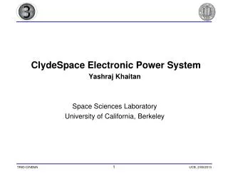
CINEMA Solar Array Design Review Yashraj Khaitan David Glaser Kevin Jenkins Chris Pasma Space Sciences Laboratory University of California, Berkeley. Solar Array Design Agenda. AGENDA Electrical Design Requirements Schematic Overview Current Calculations Issues

E N D
CINEMA Solar Array Design Review Yashraj Khaitan David Glaser Kevin Jenkins Chris Pasma Space Sciences Laboratory University of California, Berkeley
Solar Array Design Agenda AGENDA Electrical Design Requirements Schematic Overview Current Calculations Issues Developmental Plans Layer Images Mechanical Design and Assembly Panel Assembly TASC Electrical Tests Encapsulant Array Design (Time Permitting)
Solar Array Design Agenda Electrical Design
Requirements • Panel Size: Each panel covers ~ 8cm x 8cm area with 24 cells on a panel • Blocking: Blocking diodes need to be used to prevent back biasing shadowed cells • Magnetic Effects: Cells need to be wired to minimize generated magnetic torque • Monitoring: Array temperatures need to be monitored during operation.
Overview • Panel Size: The panels are 3.465” x 3.420” • Blocking: SOD-123 blocking diodes are placed on each cell pair to prevent reverse current in shadowed cells • Magnetic Effects: Diagonal routing on middle and bottom layers cancels the generated magnetic torque • Monitoring: LM135-335 is used to monitor temperatures on the board • Contacts between cell and PCB: Wide copper traces have been placed to maximize contact area. Mounting holes have been placed on the PCB for epoxy filling
Current Calculations • Via current: The current permissible in the smallest via (12mil) is 0.9618A • Trace current: The current permissible in the traces (12mil wide) is 0.5886A
Issues • Trace Currents: • Trace widths need to be adjusted to handle higher currents (672mA/Panel) • Layout software giving trouble with multiple trace widths • Testing PCB: • Jumpers have not been installed on this PCB to verify current levels of individual cell pairs or particular traces • The only way of testing current levels is to not mount the diodes and short those terminal pads • Connectors: • The connector used on each panel is a 6 pin connector and the one used on the EPS is also 6 pin • However, the EPS connects to two panels at a time
Development Plans • Prototype this design with a PCB layout company - Have quote for $520 for 10 boards • Test the board by checking current levels, temperature of cells, efficiency of cells under different operating temperatures. • Harness needs to be made to connect 6 pin terminals of two panels to a single 6 pin connector on the EPS • Interface board with the EPS to test MPPT operation
Requirements • Panel Size: Each panel covers ~ 8cm x 8cm area with 24 cells on a panel • Cells must be glued to panel with structural and electrical integrity • Cells should last for nominal 1-year mission duration
Basic Approach • Basic Approach borrowed from other projects • Custom PCB • Glue TASC Cells to PCB
Assembly Procedure Option 1 • Start with PCB, with TASC contacts ~1.5mm holes in back for structural epoxy application • Apply silver epoxy to PCB contacts • Place solar cell appropriately on PCB, allow to cure for 2 hours at 80C • Use syringe to apply Scotchweld 1838 epoxy through back-holes Option 2 Scotchweld 1838 may be applied along with silver epoxy, eliminating need for thru-holes and separate cure, if logistics allow. • Issues may include air escape and epoxy mixing After silver epoxy and Scothweld 1838 have dried • Technicians will solder top pad of each TASC rectangle to the adjacent PCB pad.
Backup Slide Electrical Performance of Silver Epoxy (Adhesive left over from THEMIS (expired)
Reference Data for Solar Cell Performance 24 pairs have been chose for first 2 panels
CV10-2500 Encapsulant • Nusil markets substance as • “for electronic and space applications requiring low outgassing and minimal volatile condensables." • for "...applications such as solar arrays where clarity and low volatility are important." • We want to do UV tests soon to determine extent of protection • Procedure: • Mix encapsulant 1:1 (by weight) and place in vacuum chamber to deaerate • Apply encapsulant to finished PCB with camel-hair brush • Thickness: "historically our satellite manufactures utilize a >0.005 " bond line." –Nusil technical sales • Allow assembly to cure 15 mins @ 150C (manufacturer specification)
Solar Array Design (If time allows) See SolidWorks Model of CINEMA