Metal-Oxide-Semiconductor (MOS)
850 likes | 1.64k Vues
Metal-Oxide-Semiconductor (MOS). EBB424E Dr. Sabar D. Hutagalung School of Materials & Mineral Resources Engineering, Universiti Sains Malaysia. MOS (Metal-Oxide-Semiconductor). Assume work function of metal and semiconductor are same. MOS materials. MOS structure.

Metal-Oxide-Semiconductor (MOS)
E N D
Presentation Transcript
Metal-Oxide-Semiconductor (MOS) EBB424E Dr. Sabar D. Hutagalung School of Materials & Mineral Resources Engineering, Universiti Sains Malaysia
MOS (Metal-Oxide-Semiconductor) Assume work function of metal and semiconductor are same.
MOS structure • Shown is the semiconductor substrate with a thin oxide layer and a top metal contact, also referred to as the gate. • A second metal layer forms an Ohmic contact to the back of the semiconductor, also referred to as the bulk. • The structure shown has a p-type substrate. • We will refer to this as an n-type MOS capacitor since the inversion layer contains electrons.
Structure and principle of operation • To understand the different bias modes of an MOS we consider 3 different bias voltages. • (1) below the flatband voltage, VFB • (2) between the flatband voltage and the threshold voltage, VT, and • (3) larger than the threshold voltage. • These bias regimes are called the accumulation, depletion and inversion mode of operation.
Structure and principle of operation • Charges in a MOS structure under accumulation, depletion and inversion conditions
Four modes of MOS operation • The four modes of operation of an MOS structure: • Flatband, • Depletion, • Inversion and • Accumulation. • Flatband conditions exist when no charge is present in the semiconductor so that the Si energy band is flat. • Surface depletion occurs when the holes in the substrate are pushed away by a positive gate voltage. • A more positive voltage also attracts electrons (the minority carriers) to the surface, which form the so-called inversion layer. • Under negative gate bias, one attracts holes from the p-type substrate to the surface, yielding accumulation
MOS capacitor- accumulation • Accumulation occurs typically for -ve voltages where the -ve charge on the gate attracts holes from the substrate to the oxide-semiconductor interface. • Depletion occurs for positive voltages. • The +ve charge on the gate pushes the mobile holes into the substrate. • Therefore, the semiconductor is depleted of mobile carriers at the interface and a -ve charge, due to the ionized acceptor ions, is left in the space charge region.
MOS capacitor- flat band • The voltage separating the accumulation and depletion regime is referred to as the flatband voltage, VFB. • The flatband voltage is obtained when the applied gate voltage equals the workfunction difference between the gate metal and the semiconductor. • If there is a fixed charge in the oxide and/or at the oxide-silicon interface, the expression for the flatband voltage must be modified accordingly.
MOS capacitor- inversion • Inversion occurs at voltages beyond the threshold voltage. • In inversion, there exists a negatively charged inversion layer at the oxide-semiconductor interface in addition to the depletion-layer. • This inversion layer is due to minority carriers, which are attracted to the interface by the positive gate voltage.
MOS Capacitance • CV measurements of MOS capacitors provide a wealth of information about the structure, which is of direct interest when one evaluates an MOS process. • Since the MOS structure is simple to fabricate, the technique is widely used. • To understand CV measurements one must first be familiar with the frequency dependence of the measurement. • This frequency dependence occurs primarily in inversion since a certain time is needed to generate the minority carriers in the inversion layer. • Thermal equilibrium is therefore not immediately obtained.
MOS Capacitance • Capacitance depends on frequency of applied signal. • If speed of variation is slow enough so that electrons can be generated by thermal generation fast enough to be created in phase with applied signal, then Cs is very large • If variation is too high a frequency, electron concentration remains fixed at the average value and capacitance depends on capacitance of depletion region
nMOS C-V characteristic of p-type Semiconductor
pMOS C-V characteristic of n-type Semiconductor
Low frequency capacitance of an nMOS capacitor. • Shown are the exact solution for the low frequency capacitance (solid line) and the low and high frequency capacitance obtained with the simple model (dotted lines). Na = 1017 cm-3 and tox = 20 nm.
(a) The threshold voltage and the ideal MOS structure (b) In practice, there are several charges in the oxide and at the oxide-semicond interface that effect the threshold voltage: Qmi = mobile ionic charge, Qot = trapped oxide charge, Qf = fixed oxide charge, Qit = charge trapped at the interface.
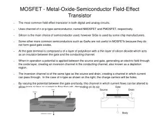
Parallel plate capacitance • An n-channel MOS transistor. The gate-oxide thickness, TOX, is approximately 100 angstroms (0.01 mm). A typical transistor length, L = 2 l. The bulk may be either the substrate or a well. The diodes represent pn-junctions that must be reverse-biased
Parallel plate capacitance • The channel and the gate form the plates of a capacitor, separated by an insulator - the gate oxide. • We know that the charge on a linear capacitor, C, is Q = C V • The channel charge, Q.
Parallel plate capacitance • At lower plate, the channel, is not a linear conductor. • Charge only appears on the lower plate when the voltage between the gate and the channel, VGC, exceeds the n-channel threshold voltage. • For nonlinear capacitor we need to modify the equation for a linear capacitor to the following: Q = C(VGC – Vt)
Parallel plate capacitance • The lower plate capacitor is resistive and conducting current, so that the VGC varies. • In fact, VGC = VGS at the source and VGC = VGS – VDS at the drain. • What we really should do is find an expression for the channel charge as a function of channel voltage and sum (integrate) the charge all the way across the channel, from x = 0 (at the source) to x = L (at the drain). • Instead we shall assume that the channel voltage, VGC(x), is a linear function of distance from the source and take the average value of the charge, which is Q = C [(VGS – Vt) – 0.5 VDS]
Parallel plate capacitance • The gate capacitance, C, is given by the formula for a parallel-plate capacitor with length L , width W , and plate separation equal to the gate-oxide thickness, Tox. • Thus the gate capacitance is C = (W L eox)/Tox = W L Cox • where eox is the gate-oxide dielectric permittivity • For SiO2 , eox ~ 3.45 x 10⁻¹¹ Fm–1, so that, for a typical gate-oxide thickness of 100 Å (= 10 nm), the gate capacitance per unit area, Cox ~ 3 fFmm–2.