Download
1 / 2
30 likes | 330 Vues
Microwave Impedance Imaging of Complex materials Zhi-Xun Shen, Stanford University, DMR 0906027.

E N D
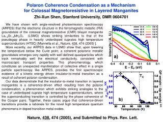
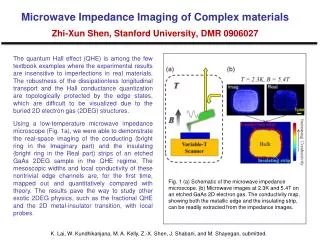
Microwave Impedance Imaging of Complex materialsZhi-Xun Shen, Stanford University, DMR 0906027 The quantum Hall effect (QHE) is among the few textbook examples where the experimental results are insensitive to imperfections in real materials. The robustness of the dissipationless longitudinal transport and the Hall conductance quantization are topologically protected by the edge states, which are difficult to be visualized due to the buried 2D electron gas (2DEG) structures. Using a low-temperature microwave impedance microscope (Fig. 1a), we were able to demonstrate the real-space imaging of the conducting (bright ring in the Imaginary part) and the insulating (bright ring in the Real part) strips of an etched GaAs 2DEG sample in the QHE regime. The mesoscopic widths and local conductivity of these nontrivial edge channels are, for the first time, mapped out and quantitatively compared with theory. The results pave the way to study other exotic 2DEG physics, such as the fractional QHE and the 2D metal-insulator transition, with local probes. Fig. 1 (a) Schematic of the microwave impedance microscope. (b) Microwave images at 2.3K and 5.4T on an etched GaAs 2D electron gas. The conductivity map, showing both the metallic edge and the insulating strip, can be readily extracted from the impedance images. K. Lai, W. Kundhikanjana, M. A. Kelly, Z.-X. Shen, J. Shabani, and M. Shayegan, submitted.
Microwave Impedance Imaging of Complex materialsZhi-Xun Shen, Stanford University, DMR 0906027 The local electrical maps contain not only fundamental importance for physics research but also pedagogical merit for the general public. We participated in the outreach program with the Latino College Preparatory Academy and the Exploratorium Teacher Institute (Fig. 2) and presented in the NSF nanoscale probing and imaging workshop. The concepts of “nano” and “spatial non-uniformity” are readily appreciated by the students and teachers. The ability to study local electrical properties without contact electrodes also attracts much interest from the industry, such as Agilent Technologies Inc. The microscope can now be configured either as a standard mode on state-of-the-art atomic-force microscope platforms for general-purpose material science research (Fig. 2), or as a customized instrument for condensed matter physics studies. Fig. 2 (Top) Lab tours for students and high school teachers. (Bottom) General-purpose microwave imaging on various samples for studying the local electrical properties.