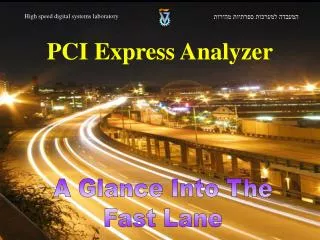
PCI Express Analyzer
High speed digital systems laboratory. המעבדה למערכות ספרתיות מהירות. PCI Express Analyzer. A Glance Into The Fast Lane. הטכניון - מכון טכנולוגי לישראל. Technion - Israel institute of technology. Analyzer Core. Final Presentation. Samuel Amir , Danny Volkind Mr. Orbach Mony.

PCI Express Analyzer
E N D
Presentation Transcript
High speed digital systems laboratory המעבדה למערכות ספרתיות מהירות PCI Express Analyzer A Glance Into The Fast Lane
הטכניון - מכון טכנולוגי לישראל Technion - Israel institute of technology Analyzer Core Final Presentation Samuel Amir , Danny Volkind Mr. Orbach Mony
High speed digital systems laboratory המעבדה למערכות ספרתיות מהירות Agenda • PCI - Express – Reminder • Link and Lane Training - Overview • Project Goals • Project features and capabilities • PCI-Express Generator - Brief
High speed digital systems laboratory המעבדה למערכות ספרתיות מהירות Agenda (cont.) • Project Block Diagram • Demonstration • Future Improvement Procedures
High speed digital systems laboratory המעבדה למערכות ספרתיות מהירות PCI - Express Reminder
High speed digital systems laboratory המעבדה למערכות ספרתיות מהירות PCI-Express Topology • Dual Simplex • Differential • Speeds of 2.5Gb/sec TX+ RX+ TX- RX- Device A Device B Ref. Clock Ref. Clock TX+ RX+ RX- TX-
Data CRC Frame Sequence Number Header Frame Transaction Transaction Layer Data Link Data Link Layer Physical Layer Physical High speed digital systems laboratory המעבדה למערכות ספרתיות מהירות Packet Formation Packet formation reflects layered architecture.
Byte Value 00H 8b/10b Encoded Byte Value High speed digital systems laboratory המעבדה למערכות ספרתיות מהירות 8/10b conversion (4.2.1) • Convert each byte to a 10bit character according to a pre-defined table. • Extra characters are used as control characters or not used. • Embedded clocking-> No need to add clock traces. • Error detection (running disparity). • DC balancing • Reduces ISI.
High speed digital systems laboratory המעבדה למערכות ספרתיות מהירות PCI Express scrambling (4.2.3) • Assures no constant pattern is transmitted. • Spread the energy transmitted in one frequency to different frequencies-> reduces EMI! (and gets FCC approval) • Only data characters are encoded. • Encoding is done using a linear feedback shift register. • Decoding is done using the same process at the receiver side.
High speed digital systems laboratory המעבדה למערכות ספרתיות מהירות Frequency Mismatch (4.2.7) How does the protocol cope with the fact that each device is feed by a different clock source? TX+ RX+ TX- RX- Device A Device B Ref. Clock Ref. Clock TX+ RX+ RX- TX-
High speed digital systems laboratory המעבדה למערכות ספרתיות מהירות Frequency Mismatch (4.2.7) Input @ 2501MHz Output @ 2500MHz Input Shift Register is filling up faster than it is emptied! Input @ 2500MHz Output @ 2501MHz Input Shift Register is emptied faster than it is filled! If we take 600ppm difference between clocks, the transmitter and receiver clocks can shift one clock every 1666 clocks!
High speed digital systems laboratory המעבדה למערכות ספרתיות מהירות Frequency Mismatch-Solution • The protocol issues a SKIP ordered set that can be skipped so that the input shift register can be partially cleared! • The SKIP ordered sets insertion time asdictated by the protocol is between 1180 and 1538 symbol times. • Calculated allowed deviance : ± 300ppm ! • This is known as “clock tolerance compensation mechanism”.
High speed digital systems laboratory המעבדה למערכות ספרתיות מהירות Link & Lane Training
High speed digital systems laboratory המעבדה למערכות ספרתיות מהירות Link and Lane Training Lane - a single set of differential RX TX pairs Link - a collection of lanes connecting two PCI-Express Devices. x1 Lane wide Link
High speed digital systems laboratory המעבדה למערכות ספרתיות מהירות Link and Lane Training (cont) Training - a process aimed at turning a collection of available lanes into a properly functioning link. • Elements established during training : • Physical Level • SERDES lock. • Symbol alignment. • Link Level link configuration • Link data rate • Link width • Etc.
High speed digital systems laboratory המעבדה למערכות ספרתיות מהירות Link and Lane Training (cont)
High speed digital systems laboratory המעבדה למערכות ספרתיות מהירות Training Ordered Sets • Group of 16 symbols. • Used During Polling State (TS1,TS2) • Establish alignment • Exchange Physical layer parameters • Not scrambled!
High speed digital systems laboratory המעבדה למערכות ספרתיות מהירות Training Ordered Sets (cont) TS1
High speed digital systems laboratory המעבדה למערכות ספרתיות מהירות Fast Training Sequence Used to re-establish bit and symbol lock when transitioning out of the LO power management state. FTS pattern
High speed digital systems laboratory המעבדה למערכות ספרתיות מהירות Skipped Ordered Set (CTC) Compensate for differences in frequencies between bit rates at two devices sharing a mutual Link (Clock Tolerance Compensation) Skipped Ordered Set pattern
High speed digital systems laboratory המעבדה למערכות ספרתיות מהירות Electrical Idle • Steady state condition • Transmitter differential pair held at fixed value • Must remain at this state at least 20nsec • Must attempt to detect a receiver within 100msec
Frame 1byte DLLP Contents 4byte Frame 1byte CRC 2byte Physical Layer Data Link Layer High speed digital systems laboratory המעבדה למערכות ספרתיות מהירות DLLP packet
Data 0-4Kbyte LCRC 4byte Frame 1byte Sequence# 2byte Header 12/16byte Frame 1byte Transaction Layer Data Link Layer Physical Layer High speed digital systems laboratory המעבדה למערכות ספרתיות מהירות TLP packet
Memory, I/O, Config, Message; Request or Completion Data Payload Indicator and 16/12B header flag Bus#, Device#, Function#, Virtual Channel Support CRC Frame Sequence Number Frame Data Fmt Type Requestor ID Rsrv Traffic Class Data Link Layer Address/Routing 16/12 Byte Transaction Layer Physical Layer Length Attr Tag Rsrv Byte Enables Requested Length or Payload Size Attributes: Snoop, Ordering Transaction Tag Reserved for future expansion First DW BE; Last DW BE High speed digital systems laboratory המעבדה למערכות ספרתיות מהירות Packet Header Header
High speed digital systems laboratory המעבדה למערכות ספרתיות מהירות Project Goals
High speed digital systems laboratory המעבדה למערכות ספרתיות מהירות Project Goal Overview • PCI-Express packets capturing at wire speed of 2.5Gbps • Selective filtering – work modes • TLP analysis – header based filtering • Simple register based user interface • RS232 accessible.
High speed digital systems laboratory המעבדה למערכות ספרתיות מהירות Project Features & Capabilities
High speed digital systems laboratory המעבדה למערכות ספרתיות מהירות Project features • Receiving PCIe communication at 2.5 Gbps. • Full line synchronization capability according to PCIe spec. • Handling of realignment and clock tolerance compensation events on the fly. • Invalid symbol filtering.
High speed digital systems laboratory המעבדה למערכות ספרתיות מהירות Project features (cont.) • Detection of and field extraction for all PCIe training sequences. • Selective descrambling of the received data. • Accumulative user-controlled counters for statistic purposes. • Data stream marking and preliminary analysis.
High speed digital systems laboratory המעבדה למערכות ספרתיות מהירות Projects features (cont.) • 6 Available work modes: • Wire Speed Capture. • Capture TS1 / TS2 • Capture DLLP • Capture TLP • Selective TLP capture
High speed digital systems laboratory המעבדה למערכות ספרתיות מהירות Projects features (cont.) • TLP filtering versatility:
High speed digital systems laboratory המעבדה למערכות ספרתיות מהירות Project features (cont.) • Storage • Fully user controlled dynamically allocated 16K x 32 memory. • Captured data is saved with preliminary analysis. • Bursts and capture events are separated allowing selective extraction.
High speed digital systems laboratory המעבדה למערכות ספרתיות מהירות Project features (cont.) • LCD Interface • Built-in LCD micro-controller implementation. • 1 Kbyte user memory for display commands. • Display file can be loaded on the fly.
High speed digital systems laboratory המעבדה למערכות ספרתיות מהירות Project features (cont.) • User Interface • RS232 serial link operating at 115.2Kbps. • Simple comm. protocol implementation allowing read and write commands accessing 32bit address space with 16bit data. • All the core features are accessible.
High speed digital systems laboratory המעבדה למערכות ספרתיות מהירות Generator - Overview • Capable of generating all PCIe traffic. • Fully user-controlled. • PCIe compatible including clock tolerance compensation simulation. • Can be set to continuous or single shot mode.
High speed digital systems laboratory המעבדה למערכות ספרתיות מהירות Generator - Overview
Transaction Data Link Physical Gigabit Receiver 1 Decryption Module 2 Physical Data Link Wrap Filter 3 Packet Filter 4 Central Controller Memory Controller 7 8 MSU Control 5 Link Assessment 6 High speed digital systems laboratory המעבדה למערכות ספרתיות מהירות Basic Block Diagram Physical Physical 4 3 7 Transaction 2 8 5 Physical 6 1
High speed digital systems laboratory המעבדה למערכות ספרתיות מהירות Top Level
High speed digital systems laboratory המעבדה למערכות ספרתיות מהירות Project Block Diagram
High speed digital systems laboratory המעבדה למערכות ספרתיות מהירות PDM – LFSR 8 bit values generated by LFSR for repeated data value of 0
High speed digital systems laboratory המעבדה למערכות ספרתיות מהירות PDM – LFSR (cont) Scrambling spectral power distribution for repeated data value of 0
High speed digital systems laboratory המעבדה למערכות ספרתיות מהירות PDM – LFSR (cont)
High speed digital systems laboratory המעבדה למערכות ספרתיות מהירות PDM – LFSR (cont)
RS232 Request Packet CRC Frame Sequence Number Frame Device B Analyzer Device A Frame CRC Completion Packet Sequence Number Frame High speed digital systems laboratory המעבדה למערכות ספרתיות מהירות Demonstration
High speed digital systems laboratory המעבדה למערכות ספרתיות מהירות Future Developments • Additional functions. • User interface development. Open Code flexibility opens the door for development
Thank You ! High speed digital systems laboratory המעבדה למערכות ספרתיות מהירות Closing Words
High speed digital systems laboratory המעבדה למערכות ספרתיות מהירות Additional information Certain images adopted from PCI-SIG PCI Express™ Architectural Overview Presented at the 2002 PCI-SIG Developers Conference and Intel Developers Forum, Fall 2001.
High speed digital systems laboratory המעבדה למערכות ספרתיות מהירות Project Development Process Semester A Semester B High Speed Communication Fundamentals Constructing Analyzer Core Building Blocks PCI Express Architecture Concepts Debugging & Testing Each block market survey Current Available Products Final Core Integration Existing Infrastructure Analyzer Core Development report Final Concept Requirements Doc