

SlideServe
Menu
Préférences
© SlideServe · v2026

PCI Express Switch

kaspar avatar
15 diapositives · 429 Views · Sep 06, 2014

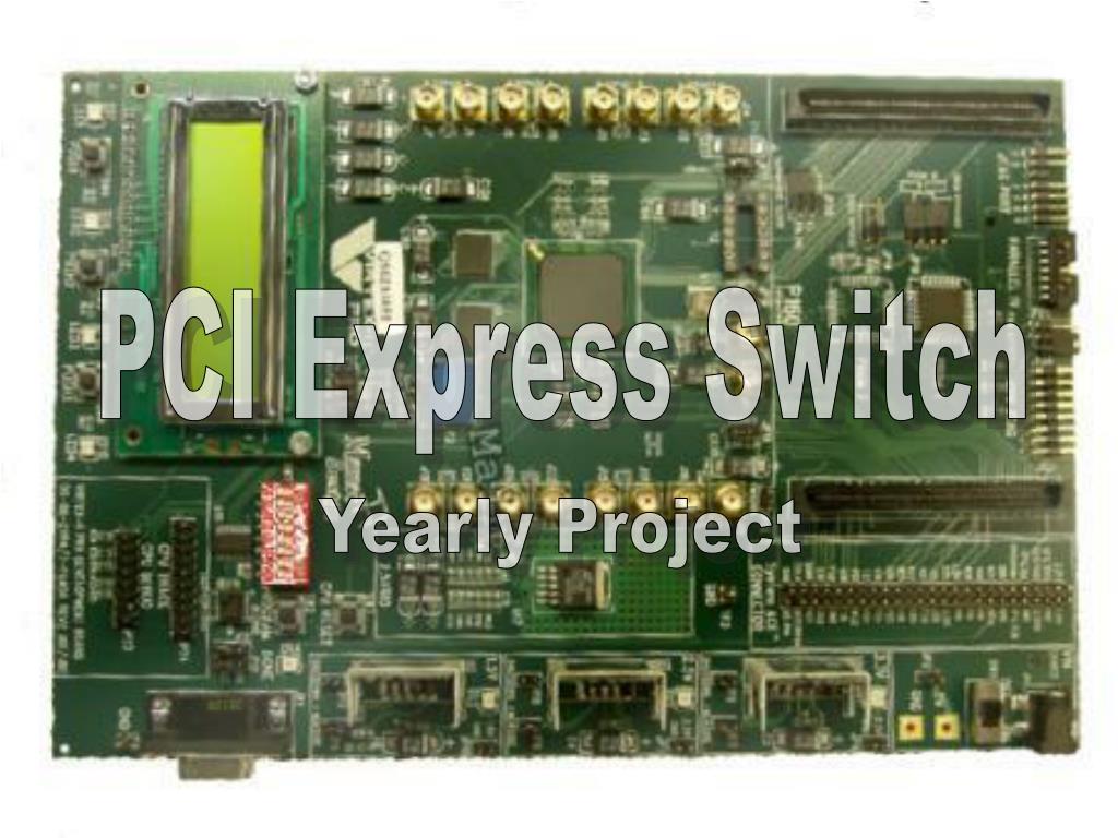
PCI Express Switch. Yearly Project. HS/DSL Project. Midterm Presentation. Implementation and Synthesis of a 3-Port PCI-Express Switch. Supervisor: Mony Orbach. Yael Grossman. Arik Krantz. Project Specifications. We will implement: 3 - port switch for PCI-Express
PCI Express Switch - slide 1
01 / 15PCI Express Switch
1 / 17

Télécharger la présentation

PCI Express Switch
Une image / un lien ci-dessous est fourni (tel quel) pour télécharger la présentation

Politique de téléchargement : le contenu du site vous est fourni TEL QUEL pour votre information et votre usage personnel ; il ne peut être vendu, concédé sous licence ni partagé sur d’autres sites sans l’accord de son auteur.Le contenu vous est fourni TEL QUEL, pour votre information et votre usage personnel uniquement. Téléchargez la présentation en cliquant sur ce lien. Lors du téléchargement, si vous ne parvenez pas à télécharger une présentation, l’éditeur a peut-être supprimé le fichier de son serveur.Pendant le téléchargement, si vous ne parvenez pas à obtenir une présentation, le fichier a peut-être été supprimé par l’éditeur.

F I N

Plus de contenu associé

Transcription de la présentation
  1. PCI Express Switch Yearly Project

  2. HS/DSL Project Midterm Presentation Implementation and Synthesis of a 3-Port PCI-Express Switch Supervisor: Mony Orbach Yael Grossman Arik Krantz

  3. Project Specifications We will implement: • 3 - port switch for PCI-Express • 1 upstream, 2 downstream full-duplex ports • Up to 2.5 Gbit/sec transfer rate • CRC support at the DLL layer • Independent packet handling per port • Packet routing between ports through lookup tables

  4. Local/Global Mechanisms • Send Queue 1 and 2 (SQ1, SQ2) Contain packets routed to current port from the other two switch ports. We have one buffer for each queue in order to prevent simultaneous memory write. • ACK/NACK Queue (ACKQ) Used to store DLLPs for each received TLP while they await sending. • Replay Buffer (RB) Contains all the packets that have been sent on the outgoing queue and have not yet received an ACK. • Send/Receive Pipelines Includes logic for incoming and outgoing packets. • Routing Mechanism Includes an independent copy of the routing table. Local • Packet Storage in Common Memory Space Enables fast packet forwarding between ports • Global Initialization at Boot Time Initialize routing tables with system layout. Global

  5. Receive Flow • This mechanism is applied per port. • It displays the sequence of actions that the switch executes on a received packet. • Packet is received on incoming lane • Packet type is determined and CRC check is performed • According to packet type (DLLP or TLP), we take appropriate action.

  6. Route packet and Enqueue (TLPs) ACK/ NACK Send Logic (TLPs) CRC Logic Block Replay Buffer Logic (DLLPs) Continue

  7. Return

  8. Return

  9. Return

  10. Return

  11. Send Flow • This mechanism is applied per port. • It displays the sequence of actions that the switch executes in order to send a packet on the outgoing lane. • The switch contains 4 buffers with packets to be sent: SQ1, SQ2, ACKQ and the Replay Buffer. • It will decide from which buffer to select the packet to be sent (if they aren’t empty), and send it on the outgoing lane.

  12. Completed Tasks Detailed design • Data flow diagram (transmitter/ receiver) for ports • Queue and buffer structure for ports • Packet handling algorithms System block design • Completed most of higher-level block design • Work in progress on lower-level blocks Preparation for VHDL coding • Learned to work with HDL designer • Learned VHDL (basic level)

  13. Semester Plan Complete design for all sub-blocks 3 weeks • Routing/lookup table mechanism • Arbitration logic • Send Queue implementation • Concurrency issues in queue access • Deal with unresolved issues such as: - Interaction with Physical Layer - Understand memory segmentation VHDL design1 week • Division of the system into interconnected entities • Definition of appropriate architecture per entity • Preparation for VHDL implementation Exam period break… 4 weeks VHDL design1 week • …continue design (and start coding).

  14. Thank You!