ECE 340 Lecture 27 P-N diode capacitance
320 likes | 945 Vues
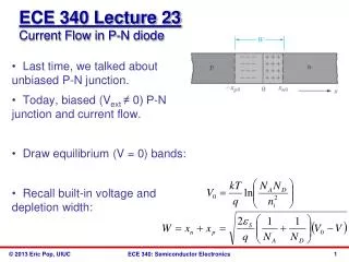
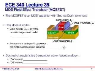
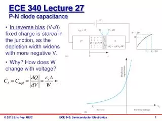
ECE 340 Lecture 27 P-N diode capacitance. In reverse bias (V<0) fixed charge is stored in the junction, as the depletion width widens with more negative V. Why? How does W change with voltage?. If we measure and plot 1/C J 2 vs. V, I can get __________.

ECE 340 Lecture 27 P-N diode capacitance
E N D
Presentation Transcript
ECE 340 Lecture 27P-N diode capacitance • In reverse bias (V<0) fixed charge is stored in the junction, as the depletion width widens with more negative V. • Why? How does W change with voltage?
Ex: Diode with area 100x100 μm2, slope of (1/CJ)2 vs. V is -2x10²³ F-2V-1, and intercept is 0.84 V. If NA >> ND, find the two sides’ doping.
In forward bias (V>0) excess minority carriers are stored in the quasi-neutral regions of the p-n diode. In n-side (note zero of x-axis redefined to xn0 = 0): Where Δpn(xn) = and Lp = In p-side (note zero of x-axis redefined to xp0 = 0):
Diffusion capacitance for holes in n-side: • Where ℓn = ________________ • And pn = _________________ • Keep in mind that in general CJ(V) = Cdepl + Cdiff • “Long” diode = _______________________ • “Short” diode = _______________________
We’ve (nearly) exhausted the p-n junction. Now we know: 1) Why and how it conducts current (forward, reverse) 2) How to calculate depletion width, field, built-in voltage 3) How diodes break down 4) How diodes store charge as capacitors 5) How to make an LED or photodiode
Two diode applications in optoelectronics: • Photodiode or solar cell 2) Light-emitting diode (LED)
ECE 340 Lecture 28-29P-N optoelectronics; photodetectors, solar cells, LEDs Recall: Si is great (cheap, good SiO2 insulator) for high complexity digital & cheap analog circuits What if we want: High-speed (10s GHz – 1 THz) analog amplifiers; Optical receivers, emitters (LEDs, lasers) Look at other semiconductors with BETTER mobility and light emission / absorption properties (“custom” EG).
Another thing to keep in mind: • Direct band gap (EG) • Indirect band gap (EG) • Ball-and-stick lattice picture: • Band diagram picture: • Remember: EG = hf = hc/λ; numerically EG(eV) = 1.24/λ(μm)
We now focus mostly on direct band gap semiconductors like GaAs, InP and their alloys: • Note, we can vary alloy composition (e.g. InxGa1-xAs) and get different _________ and _____________ • Getting same lattice constant as the substrate (GaAs or InP) is important to minimize lattice defects in a device. • Generally, assume lattice constant (a) and band gap (EG) vary linearly with alloy fraction (x)
We know p-n junction can be used to: • Emit light (EHP recombination at ___________ bias) • Absorb light (EHP generation at ___________ bias) • Minority & majority carriers recombine and emit light • In the ________________ region (WD) • Within a _______________ length (Ln, Lp) in n- and p-sides
Can we control & improve p-n light emission / absorption? • Use p-n heterojunction, i.e. make depletion region in a material with _____________ EG • Use p-i-n diode by making depletion region intrinsic (“i”) to enlarge depletion region W
What are the current & voltage in an illuminated junction? 1) Note: need illumination photon energy hf > EG 2) Assume quantum efficiency Q.E. = 1 = one EHP created for every incoming photon • For example, if EHP generation is gop = 1017 EHPs/cm3/s • What is the optically generated current in a diode?
How does the photogenerated current add (or subtract) to the current already induced by the diode voltage? • Short-circuit current: external V = 0 Isc = ____ • Open-circuit voltage: external I = 0 Voc = ____ • This is a photovoltaic effect.
How fast is the photodiode speed (response frequency)? fmax = …
Ex: Photodiode Design. Consider a p-i-n photodiode (see Fig. 8-7), with “i” region made of InxGa1-xAs (see Fig. 1-13). Design stoichiometry “x” and thickness of the “i” region (Wi) to enable response at 1.3 μm wavelength, up to 20 GHz signals. Assume fields are sufficiently high to reach vsat ≈ 107 cm/s in the “i” region. Name at least one design constraint on the “p” and “n” regions of this photodiode. You may assume the lattice constant and band gap of InxGa1-xAs vary linearly with composition “x”.
Optical fiber communications why use wavelengths of 1.3 or 1.55 μm? • Minimum _____________ • Minimum _____________
Semiconductor lasers vs. LEDs: • Strong fwd. bias, population inversion • Recombination region + resonant cavity (length L, between semi-reflective mirrors) • Stimulated emission at λ = 2L/m resonant modes between mirrors in laser cavity
(also see Fig. 8.10 in your textbook) http://www.infographicsshowcase.com/from-radio-receivers-to-led-flashlights-an-led-odyssey/coast-led-timeline/