ECE 546 Lecture 03 Resistance, Capacitance, Inductance
680 likes | 1.12k Vues
ECE 546 Lecture 03 Resistance, Capacitance, Inductance. Spring 2014. Jose E. Schutt-Aine Electrical & Computer Engineering University of Illinois jschutt@emlab.uiuc.edu. What is Extraction?.

ECE 546 Lecture 03 Resistance, Capacitance, Inductance
E N D
Presentation Transcript
ECE 546 Lecture 03 Resistance, Capacitance, Inductance Spring 2014 Jose E. Schutt-Aine Electrical & Computer Engineering University of Illinois jschutt@emlab.uiuc.edu
What is Extraction? Process in which a complex arrangement of conductors and dielectric is converted into a netlist of elements in a form that is amenable to circuit simulation. Need Field Solvers
Electromagnetic Modeling Tools We need electromagnetic modeling tools to analyze: Transmission line propagation Reflections from discontinuities Crosstalk between interconnects Simultaneous switching noise So we can provide: Improved design of interconnects Robust design guidelines Faster, more cost effective design cycles
Field Solvers – History 1960s Conformal mapping techniques Finite difference methods (2-D Laplace eq.) Variational methods 1970s Boundary element method Finite element method (2-D) Partial element equivalent circuit (3-D) 1980s Time domain methods (3-D) Finite element method (3-D) Moment method (3-D) rPEEC method (3-D) 1990s Adapting methods to parallel computers Including methods in CAD tools
Categories of Field Solvers • Method of Moments (MOM) • Application to 2-D Interconnects • Closed-Form Green’s Function • Full-Wave and FDTD • Parallel FDTD • Applications
Capacitance Relation: Q = Cv Q: charge stored by capacitor C: capacitance v: voltage across capacitor i: current into capacitor
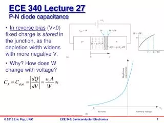
A : area e : permittivity o Capacitance For more complex capacitance geometries, need to use numerical methods
Capacitance Calculation Once the charge distribution is known, the total charge Q can be determined. If the potential f=V, we have Q=CV To determine the charge distribution, use the moment method
METHOD OF MOMENTS Operator equation L(f) = g L= integral or differential operator f = unknown function g = known function Expand unknown function f
METHOD OF MOMENTS in terms of basis functions fn, with unknown coefficients anto get Finally, take the scalar or inner product with testing of weighting functions wm: Matrix equation
METHOD OF MOMENTS Solution for weight coefficients
Moment Method Solution Green’s function G: LG = d
Basis Functions Subdomain bases Testing functions often (not always) chosen same as basis function.
Conducting Plate s = charge density on plate
Conducting Plate Setting f = V on plate for |x| < a; |y| < a Capacitance of plate:
Conducting Plate Basis function Pn Representation of unknown charge
Conducting Plate Matrix equation: Matrix element:
Parallel Plates Using N unknowns per plate, we get 2N 2N matrix equation: Subscript ‘t’ for top and ‘b’ for bottom plate, respectively.
Parallel Plates Matrix equation becomes Solution: Capacitance Using Ds=4b2 and all elements of
Inductance Relation:Y = Li Y: flux stored by inductor L: inductance i: current through inductor v: voltage across inductor
Total flux linked Inductance = Current Inductance Magnetic Flux
2-D Isomorphism Electrostatics Magnetostatics Consequence: 2D inductance can be calculated from 2D capacitance formulas
2-D N-line LC Extractor using MOM • Symmetric signal traces • Uniform spacing • Lossless lines • Uses MOM for solution
Output from MoM Extractor Capacitance (pF/m) 118.02299 -8.86533 -0.03030 -0.00011 -0.00000 -8.86533 119.04875 -8.86185 -0.03029 -0.00011 -0.03030 -8.86185 119.04876 -8.86185 -0.03030 -0.00011 -0.03029 -8.86185 119.04875 -8.86533 -0.00000 -0.00011 -0.03030 -8.86533 118.02299 Inductance (nH/m) 312.71680 23.42397 1.83394 0.14361 0.01128 23.42397 311.76042 23.34917 1.82812 0.14361 1.83394 23.34917 311.75461 23.34917 1.83394 0.14361 1.82812 23.34917 311.76042 23.42397 0.01128 0.14361 1.83394 23.42397 312.71680
RLGC: Formulation Method • Reference • K. S. Oh, D. B. Kuznetsov and J. E. Schutt-Aine, "Capacitance Computations in a Multilayered Dielectric Medium Using Closed-Form Spatial Green's Functions," IEEE Trans. Microwave Theory Tech., vol. MTT-42, pp. 1443-1453, August 1994.
Optional Top Ground Plane y=d Nd e m , N Nd o d y=d Nd-1 y=d 2 y e m , 2 2 o y=d 1 e m 1 x , 1 o y=0 Bottom Ground Plane Multilayer Green's Function
Extraction Program: RLGC RLGC computes the four transmission line parameters, viz., the capacitance matrix C, the inductance matrix L, the conductance matrix G, and the resistance matrix R, of a multiconductor transmission line in a multilayered dielectric medium. RLGC features the following list of functions:
RLGC – Multilayer Extractor • Features • Handling of dielectric layers with no ground plane, either top or bottom ground plane (microstrip cases), or both top and bottom ground planes (stripline cases) • Static solutions are obtained using the Method of Moment (MoM) in conjunction with the recently-developed closed-form Green’s functions: one of the most accurate and efficient methods for static analysis • Modeling of dielectric losses as well as conductor losses (including ground plane losses • The resistance matrix R is computed based on the current distribution - more accurate than the use of any closed-form formulae • Both the proximity effect and the skin effect are modeled in the resistance matrix R. • Computes the potential distribution • Handling of an arbitrary number of dielectric layers as well as an arbitrary number of conductors. • The cross section of a conductor can be arbitrary or even be infinitely thin • Reference • K. S. Oh, D. B. Kuznetsov and J. E. Schutt-Aine, "Capacitance Computations in a Multilayered Dielectric Medium Using Closed-Form Spatial Green's Functions," IEEE Trans. Microwave Theory Tech., vol. MTT-42, pp. 1443-1453, August 1994.
RLGC – General Topology Three conductors in a layered medium. All conductor dimensions and spacing are identical. The loss tangents of the lower and upper dielectric layers are 0.004 and 0.001respectively, the conductivity of each line is 5.8e7 S/m, and the operating frequency is 1 GHz
3-Line Capacitance Results Capacitance Matrix (pF/m) Delabare et al. RLGC Method
3D Inductance Calculation Loop Inductance QUESTION: Can we associate inductance with piece of conductor rather than a loop? PEEC Method
Partial Inductance (PEEC) Approach QUESTION: Can we associate inductance with piece of conductor rather than a loop? DEFINITION OF PARTIAL INDUCTANCE
Circuit Element K [K]=[L]-1 • Better locality property • Leads to sparser matrix • Diagonally dominant • Allows truncation of far off-diagonal elements • Better suited for on-chip inductance analysis
Package Inductance & Capacitance ComponentCapacitanceInductance (pF) (nH) 68 pin plastic DIP pin† 4 35 68 pin ceramic DIP pin†† 7 20 68 pin SMT chip carrier † 2 7 † No ground plane; capacitance is dominated by wire-to-wire component. †† With ground plane; capacitance and inductance are determined by the distance between the lead frame and the ground plane, and the lead length.
Package Inductance & Capacitance ComponentCapacitanceInductance (pF) (nH) 68 pin PGA pin†† 2 7 256 pin PGA pin†† 5 15 Wire bond 1 1 Solder bump 0.5 0.1 † No ground plane; capacitance is dominated by wire-to-wire component. †† With ground plane; capacitance and inductance are determined by the distance between the lead frame and the ground plane, and the lead length.
Metallic Conductors Metal Conductivity s(W-1m-110-7) Silver 6.1 Copper 5.8 Gold 3.5 Aluminum 1.8 Tungsten 1.8 Brass 1.5 Solder 0.7 Lead 0.5 Mercury 0.1
Dielectrics contain charges that are tightly bound to the nuclei Charges can move a fraction of an atomic distance away from equilibrium position Electron orbits can be distorted when an electric field is applied Dielectrics
Charge density within volume is zero Surface charge density is nonzero Dielectrics D=eo(1+e)E=eE
Dielectric Materials MaterialConductivity (W-1-m-1) Germanium 2.2 Silicon 0.0016 Glass 10-10-10-14 Quartz 0.510-17
Dielectric Materials Materialerv(cm/s) Polyimide 2.5-3.5 16-19 Silicon dioxide 3.9 15 Epoxy glass (FR4) 5.0 13 Alumina (ceramic) 9.5 10
MaterialConductivity (W-1 m-1) Germanium 2.2 Silicon 0.0016 Glass 10-10 - 10-14 Quartz 0.5 x 10⁻¹⁷ Loss TANGENT : tand = s w e Conductivity of Dielectric Materials e = er + jei
Combining Field and Circuit Solutions Field Solution Network Description Macromodel Generation Circuit Simulation • Bypass extraction procedure through the use of Y, Z, or S parameters (frequency domain)
Full-Wave Methods Faraday’s Law of Induction Ampère’s Law Gauss’ Law for electric field Gauss’ Law for magnetic field FDTD: Discretize equations and solve with appropriate boundary conditions
z y E y x H z E x E x E z E z E y H x H y H y E y H x E z E x E x H z E y Finite Difference Time Domain (FDTD) Space Discretization
z y E y x H z E x E x E z E z E y H x H y H y E y H x E z E x E x H z E y FDTD – Yee Algorithm
E y E x H z 2D-FDTD y x