Download
1 / 16
190 likes | 356 Vues
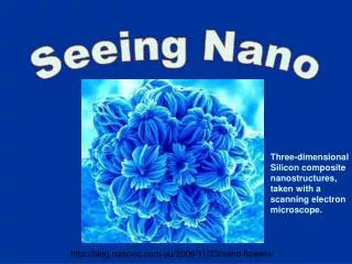
Seeing Nano. Three-dimensional Silicon composite nanostructures, taken with a scanning electron microscope. http://blog.nanovic.com.au/2006/11/23/nano-flowers/. http://www.daviddarling.info/images/Lippershey.jpg. http://www.aps.org/publications/apsnews/200403/images/microscope_inventor.jpg.

E N D
Seeing Nano Three-dimensional Silicon composite nanostructures, taken with a scanning electron microscope. http://blog.nanovic.com.au/2006/11/23/nano-flowers/
http://www.daviddarling.info/images/Lippershey.jpg http://www.aps.org/publications/apsnews/200403/images/microscope_inventor.jpg A Brief History In the history of the human race, we have developed many instruments to help us see things which are invisible to the human eye. First telescope - ~1600 developed by a Dutch spectacle maker named Hans Lippershey First compound microscope - ~1590, developed by Dutch spectacle makers; Zaccharias Janssen and his son Hans. Lippershey Janssen
Optical Microscopes Optical (light) microscopes Scale of about 200 nm.3 Not small enough for nanotechnology http://www.microscopeworld.com/MSWorld/images/scopeparts.jpg
Types of Microscopes4 • Scanning Electron Microscopes • Shoot a thin electron beam at surface and look at the reflection of those electrons • Map topography (surface) of sample • Transmission Electron Microscopes • Pass electrons through sample whose interactions produce an image on a screen • Require careful sample preparation • Scanning Probe Microscopes • Use a physical probe to either touch or come close to touching the sample • Mostly give information about the topography of the sample
SEM http://images.google.com/imgres?imgurl=http://www.rpi.edu/dept/materials/COURSES/NANO/shaw/BigSEM.gif&imgrefurl=http://www.rpi.edu/dept/materials/COURSES/NANO/shaw/Page5.html&h=675&w=621&sz=18&hl=en&start=8&um=1&tbnid=MEIi0w9m33rDjM:&tbnh=138&tbnw=127&prev=/images%3Fq%3DSEM%26um%3D1%26hl%3Den%26rlz%3D1T4SUNA_enUS222US254%26sa%3DN
TEM http://images.google.com/imgres?imgurl=http://www.rpi.edu/dept/materials/COURSES/NANO/shaw/BigSEM.gif&imgrefurl=http://www.rpi.edu/dept/materials/COURSES/NANO/shaw/Page5.html&h=675&w=621&sz=18&hl=en&start=8&um=1&tbnid=MEIi0w9m33rDjM:&tbnh=138&tbnw=127&prev=/images%3Fq%3DSEM%26um%3D1%26hl%3Den%26rlz%3D1T4SUNA_enUS222US254%26sa%3DN
SPM http://www.mtholyoke.edu/~menunez/ResearchPage/AFM_mechanism.gif
http://gsc.nrcan.gc.ca/labs/ebeam/images/sem8.jpg Electron Microscope Images TEM Fly Head SEM Fly Head http://www.optics.rochester.edu/workgroups/cml/opt307/spr05/chris/fly_eye_anaglyph_great2.jpg
Atomic Force Microscope • A type of SPM • Resolution of fractions of a nanometer • Uses a cantilever with a carbon nanotube tip or similar object for probe • Has three modes for data collection AFM Cantilever and Tip
Three Modes of AFM5 • Static Mode • Drags tip of probe across surface • Friction causes deterioration of tip • Dynamic or Tapping Mode • Cantilever is oscillated at a resonance frequency • Amplitude of oscillation is used to determine topography • Force Spectroscopy • Measures the magnetic field within a sample
AFM Images • Silicon • 77 pm resolution http://www.physik.uni-regensburg.de/forschung/giessibl/fjg/imagegallery/afmimages/AFM-image-silicon-111-tip-19052003053031.jpg
Graphite • 2 x 2 nm2 http://images.google.com/imgres?imgurl=http://www.physik.uni-regensburg.de/forschung/giessibl/fjg/imagegallery/afmimages/afm-image-graphite.jpg&imgrefurl=http://www.physik.uni-regensburg.de/forschung/giessibl/fjg/imagegallery/afmimages/afmimages_e.shtml&h=1765&w=1771&sz=2369&hl=en&start=18&um=1&tbnid=JphyWpgBLXnguM:&tbnh=149&tbnw=150&prev=/images%3Fq%3DAFM%26um%3D1%26hl%3Den%26rlz%3D1T4GGIH_enUS270US285%26sa%3DN
Chromosome http://www.nanopicoftheday.org/images/ChromosomeAFM.jpg
CD-ROM cd-rom http://upload.wikimedia.org/wikipedia/commons/thumb/9/9d/Afm_cd-rom.jpg/753px-Afm_cd-rom.jpg
Bromine atoms http://images.google.com/imgres?imgurl=http://www.wired.com/images/slideshow/2008/02/nano_microscope/07_bromine_atoms.jpg&imgrefurl=http://www.wired.com/science/discoveries/multimedia/2008/02/nano_gallery_jmm%3Fslide%3D7&h=580&w=580&sz=107&hl=en&start=2&um=1&tbnid=iuBVY9_hGCIZQM:&tbnh=134&tbnw=134&prev=/images%3Fq%3Dbromine%2Bnano%26um%3D1%26hl%3Den%26rlz%3D1T4GGIH_enUS270US285
Bibliography • 1 http://www.omni-optical.com/telescope/ut104.htm • 2 http://inventors.about.com/od/mstartinventions/a/microscope.htm • 3 http://hypertextbook.com/facts/1999/GeetikaKumar.shtml • 4 http://en.wikipedia.org/wiki/Microscope • 5 http://en.wikipedia.org/wiki/Atomic_force_microscope