Download
1 / 11
110 likes | 322 Vues
X-ray photoemission spectroscopy study on III-Nitride films. Bo Chen Department of Physics Boston University April 29, 2009. Outline. III-Nitride films (optoelectronic materials, their electronic structure not fully measured) Synchrotron-radiation based spectroscopies

E N D
X-ray photoemission spectroscopy study on III-Nitride films Bo Chen Department of Physics Boston University April 29, 2009
Outline • III-Nitride films (optoelectronic materials, their electronic structure not fully measured) • Synchrotron-radiation based spectroscopies Angle Resolved Photoemission Spectroscopy (ARPES) • ARPES study on the charge accumulation for wurtzite InN films
Wurtzite InN films: Crystal Structure and Brillouin Zone • The Wurtzite III-Nitride structure has a hexagonal unit cell • c/a = 1.633, two hexagonal sublattices, coordination number 4 • Bulk and surface Brillouin zones are hexagonal • ΓΣM, ΓTK and ΓΔA directions
Calculated Band Structure for Bulk InN A D G H K L T S M I. Mahboob, T. D. Veal, L. F. J. Piper, C. F. McConville, Hai Lu, W. J. Schaff, F. Bechstedt, and J. Furthmüller, Phys. Rev. B 69, 201307 (2004) • The conduction band minimum (CBM) at the Γ-point is muchlower than the conduction band edge at other points in k-space. • The conduction band, valence bands (heavy-hole, light-hole, and split-off bands) at Γ-point
Charge Accumulation in Wurtzite InN films Concept: Electrons accumulate in the near-surface region for certain semiconductors. Physics: Donor-type surface states cause downward band bending. The Fermi level lies in the conduction band in the accumulation layer (8 nm). Model: A 1D quantum well in the direction perpendicular to the surface and 2D electron gas in the plane parallel to the surface .
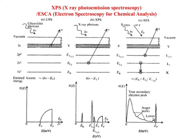
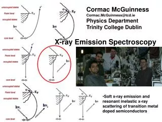
X-ray photoemission • X-ray photoemission spectroscopy (XPS) is also called Electron Spectroscopy for Chemical Analysis (ESCA). Kai Siegbahn developed the instrumentation and theory of ESCA. (Nobel Prize in Physics in 1981) • The energy and the component of the momentum parallel to the surface are conserved. • The Einstein equation: EB = hν–KE–Фsp Measuring thekinetic energy of emitted electrons gives the binding energy of electronsin the sample.
Angle Resolved Photoemission Spectroscopy (ARPES) Momentum conservation parallel to the surface gives: ARPES measures thekinetic energy and the number of emitted electrons at different emission angles and gives the energy dispersion and the Fermi surface.
ARPES measurement of Intrinsic Quantum Well States on InN Photocurrent intensity map of states along GSM, in the surface plane. hn = 69 eV; sample @ 177 K. 300°C anneal in UHV for 30 minutes. Two well-resolved, nested bands L. Colakerol et al, Phys. Rev. Lett. 97, 237601 (2006)
Fermi Surface and Constant Energy Contours from Quantum Well States on InN (a) Two well defined circular concentric structures
Conclusion • In summary, we have discussed a solid state technology of measuring the electronic structure of III-nitride films using synchrotron-radiation based spectroscopies.
Reference • 1. Gallium Nitride (GaN), J. I. Pankove, T. D. Moustakas, Semiconductors and Semimetals 50 (San Diego : Academic Press, c1998) • 2. Wide Band-Gap Semiconductors, edited by T. D. Moustakas, J. I. Pankove, and Y. Hamakawa, MRS Symposia Proceedings No. 242 (Materials Research Society, Pittsburgh, 1992). • 3. F. A. Ponce and D. P. Bour, Nature (London) 386, 351 (1997). • 4. I. Mahboob, T. D. Veal, L. F. J. Piper, C. F. McConville, Hai Lu, W. J. Schaff, F. Bechstedt, and J. Furthmüller, Phys. Rev. B 69, 201307 (2004) • 5. “Surface Analysis – The Principal Techniques”, J. C. Vickerman, Chapter 2-4, John Wiley & Sons Ltd. (1997) • 6. K. E. Smith and S. D. Kevan, Prog. Solid State Chem. 21, 49 (1991); Angle Resolved Photoemission, edited by S. D. Kevan (Elsevier, Amsterdam, 1991). • 7. S.S. Dhesi, C.B. Stagarescu, K.E. Smith, D. Doppalapudi, R. Singh and T.D. Moustakas, Phys. Rev. B 56, 10271 (1997) • 8. L. Colakerol, T.D. Veal, H.-K. Jeong, L. Plukinski, A. DeMasi, S. Wang, Y. Zhang, L.F.J. Piper, P.H. Jefferson, A. Fedorov, T.C. Chen, T. D. Moustakas, C.F. McConville, and K.E. Smith, Phys. Rev. Lett. 97, 237601 (2006). • 9. I. Mahboob, T. D. Veal, C. F. McConville, H. Lu, and W. J. Schaff, Phys. Rev. Lett. 92, 036804 (2004). • 10. L. Ö. Olsson, C. B. M. Andersson, M. C. Håkansson, J. Kanski, L. Ilver, and U. O. Karlsson, Phys. Rev. Lett. 76, 3626 (1996) • 11. K. Siegbahn et al. , ESCA: atomic, molecular and solid state structure studied by means of electron spectroscopy, Nova Acta Regiae Societatis Scientiarum Upsaliensis, Ser. IV, 20, 5-282 (1967).