Download
1 / 31
481 likes | 1.26k Vues
Chapter 4 Clean room, wafer cleaning and gettering. Introduction. Clean room. Wafer cleaning. Gettering. Measurement methods. NE 343: Microfabrication and thin film technology Instructor: Bo Cui, ECE, University of Waterloo; http://ece.uwaterloo.ca/~bcui/

E N D
Chapter 4 Clean room, wafer cleaning and gettering Introduction. Clean room. Wafer cleaning. Gettering. Measurement methods. NE 343: Microfabrication and thin film technology Instructor: Bo Cui, ECE, University of Waterloo; http://ece.uwaterloo.ca/~bcui/ Textbook: Silicon VLSI Technology by Plummer, Deal and Griffin
Effect of defect and contamination on semiconductor industry LLS: localized light scatters (use laser to detect and count particles) GOI: gate oxide integrity, by electrical measurement Requirement different for DRAM and logic chip, due to greater gate insulator area on DRAM chip. 109/cm2 0.0001% monolayer Importance of unwanted impurities increases with shrinking geometries of devices. 75% of the yield loss is due to defects caused by particles (1/2 of the min feature size).
Type of contaminants Contaminants may consist of particles, organic films, photoresist, heavy metals or alkali ions. Modern IC factories employ a three tiered approach to controlling unwanted impurities: clean factories wafer cleaning gettering
Effects on MOSFET: two examples MOSFET threshold voltage is given by: If tox=10nm, then a 0.1V Vth shift can be caused by Na+ or K+of QM=2.151011 ions/cm2 (<0.1% monolayer or 10ppm in the oxide). 0=8.8510-12F/m, ox=3.9 For MOS DRAM, refresh time of several msec requires a generation lifetime of This requires trap density Nt1012/cm3, or 0.02ppb (1012/(51022)=0.02ppb). ( is trap capture cross-section, vth is minority carrier thermal velocity; Vth107cm/sec, 10-15cm-2) Deep-level traps (Cu, Fe, Au etc.) pile up at the surface where the devices are located. This causes leak current. Need refresh/recharge the MOS capacitor. DRAM: Dynamic Random Access Memory
Effects of cleaning on thermal oxidation Residual contaminants affect kinetics of processes, here oxidation.
Particle contaminants Particle sources: air, people, equipment and chemicals. A typical person emits 5-10 million particles per minute. Particle density (number/ml) for ULSI grade chemicals ULSI: ultra-large-scale integration
Ion implantation Dry etching Photoresist removal Fe Ni Cu Wet oxidation 9 10 11 12 13 Log (concentration/cm2) Metal contamination Sources: chemicals, ion implantation, reactive ion etching, resist removal, oxidation. Effects: defects at interface degrade device; leads to leak current of p-n junction, reduces minority carrier life time. Fe, Cu, Ni, Cr, W, Ti… Na, K, Li…
Chapter 4 Clean room, wafer cleaning and gettering Introduction. Clean room. Wafer cleaning. Gettering. Measurement methods. NE 343 Microfabrication and thin film technology Instructor: Bo Cui, ECE, University of Waterloo Textbook: Silicon VLSI Technology by Plummer, Deal and Griffin
Clean factory is the first approach against contamination Modern IC factories employ a three tiered approach to controlling unwanted impurities: clean factories wafer cleaning gettering Clean factory Wafer cleaning Gettering
Clean room • Factory environment is cleaned by: • HEPA filters and recirculation for the air. • “Bunny suits” for workers. • Filtration of chemicals and gases. • Manufacturing protocols. • HEPA: High Efficiency Particulate Air • HEPA filters composed of thin porous sheets of ultrafine glass fibers (<1m diameter). • It is 99.97% efficient at removing particles from air. • Room air forced through the filter at 50cm/sec. • Large particles trapped, small ones stick to the fibers due to electrostatic forces. • The exit air is typically better than class 1.
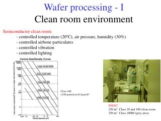
Class of a clean room • Air quality is measured by the “class” of the facility. • Class 1-100,000 mean number of particles, greater than 0.5m, in a cubit foot of air. • A typical office building is about class 100,000. • The particle size that is of most concern is 10nm – 10m. Particles <10nm tend to coagulate into large ones; those >10m are heavy and precipitate quickly. • Particles deposit on surfaces by Brownian motion (most important for those <0.5m) and gravitational sedimentation (for larger ones). Particle diameter (m) by definition
Particle contamination and yield • Generally, particles on the order of the technology minimum features size or larger will cause defect. • 75 yield loss in modern VLSI fabrication facilities is due to particle contamination. • Yield models depend on information about the description of particles. • Particles on the order of 0.1-0.3m are the most troublesome: larger particles precipitate easily; smaller one coagulate into larger particles.
Chapter 4 Clean room, wafer cleaning and gettering Introduction. Clean room. Wafer cleaning. Gettering. Measurement methods. NE 343 Microfabrication and thin film technology Instructor: Bo Cui, ECE, University of Waterloo Textbook: Silicon VLSI Technology by Plummer, Deal and Griffin
Modern wafer cleaning • Cleaning involves removing particles, organics and metals from wafer surfaces. • Particles are largely removed by ultrasonic agitation during cleaning. • Organics (photoresist) are removed in O2 plasma or in H2SO4/H2O2 (Piranha) solutions. • The “RCA clean” is used to remove metals and any remaining organics. A cassette of wafers Typical person emit 5-10 million particle per minute. Most modern IC plants use robots for wafer handling.
Standard RCA cleaning procedure RCA clean is “standard process” used to remove organics, heavy metals and alkali ions. Ultrasonic agitation is used to dislodge particles. SC: Standard Cleaning RCA: Radio Corporation of America, now makes TV, stereos… and all contaminants on top of it, but induces H passivated surface (bad) Less NH4OH will reduce surface roughness not removed by SC-1 DI water: de-ionized water HF dip added to remove oxide
Standard cleaning (SC) • SC-1: • NH4OH(28%):H2O2(30%):H2O=1:1:5- 1:2:7; 70-80C, 10min, high pH. • Oxidize organic contamination (form CO2, H2O…) • Form complex such as Cu(NH3)4+2with metals (IB, IIB, Au, Ag, Cu, Ni, Zn, Cd, Co, Cr). • Slowly dissolve native oxide and grow back new oxide, which removes particles on oxide. • But NH4OHetches Si and make the surface rough, thus less NH4OH is used today. • SC-2: • HCl(73%):H2O2(30%):H2O=1:1:6 - 1:2:8; 70 - 80C; 10min, low pH. • Remove alkali ions and cations like Al+3, Fe+3and Mg+2that form NH4OH insoluble hydroxides in basic solutions like SC-1. • These metals precipitate onto wafer surface in the SC-1 solution, while they form soluble complexes in SC-2 solution. • SC-2 also complete the removal of metallic contaminates such as Au that may not have been completely removed by SC-1 step.
Principles of metal cleaning If we have a water solution with a Si wafer and metal atoms and ions, two reactions take place. The two reactions will proceed in opposite directions, one providing electrons, which will then be consumed by the other (forming an oxidation/reduction couple). In this couple, the stronger reaction will dominate. Generally, (2) is driven to the left and (1) to the right so that SiO2 is formed and M plates out on the wafer. Good cleaning solutions drive (2) to the right since M+ is soluble and will be desorbed from the wafer surface. (1) (2)
Principles of metal cleaning The strongest oxidants are at the bottom (H2O2 and O3). These reactions go to the left, grabbing electrons and forcing (2) in previous slide to the right. Fundamentally the RCA clean works by using H2O2 as a strong oxidant. Reaction goes to the left
Ultrasonic cleaning and DI water • RCA cleaning with ultrasonic agitation is more effective in removing particles. • Ultrasonic cleaning: • Highly effective for removing surface contaminants • Mechanical agitation of cleaning fluid by high-frequency vibrations (between 20 and 45 kHz) to cause cavitation - formation of low pressure vapor bubbles that scrub the surface. • Higher frequencies (>45kHz) form smaller bubbles, thus less effective. • However, megasonic (1MHz) cleaning is also found effective in particle removal. DI (de-ionized) water is used for wafer cleaning. One monitors DI water by measuring its resistivity, which should be >18Mcm. H2O H++OH- [H+]=[OH-] = 6x10-13cm-3 Diffusivity of: H+ ≈ 9.3x10⁻⁵cm2s-1µH+=qD/kT=3.59cm2V-1s-1 of : OH- ≈ 5.3x10⁻⁵cm2s-1µOH-=qD/kT=2.04cm2V-1s-1 Einstein relation: µ=qD/kT, http://en.wikipedia.org/wiki/Einstein_relation_%28kinetic_theory%29
Other cleaning methods Ohmi cleaning: room temperature, fewer chemicals • Dry (vapor phase) cleaning: • Energy may come from plasma, ion beam, short-wavelength (UV) radiation or heating. • HF/H2Ovapor cleaning • UV-ozone cleaning (UVOC) • H2/Ar plasma cleaning • Thermal cleaning
Chapter 4 Clean room, wafer cleaning and gettering Introduction. Clean room. Wafer cleaning. Gettering. Measurement methods. NE 343 Microfabrication and thin film technology Instructor: Bo Cui, ECE, University of Waterloo Textbook: Silicon VLSI Technology by Plummer, Deal and Griffin
Gettering • For the alkali ions, gettering generally uses dielectric layers on the topside; PSG for trapping, or Si3N4 layer for blocking them from getting into the device region. • For metal ions, gettering generally uses traps on the wafer backside or in the wafer bulk. Here gettering works because the metals (Au…) do not “fit” in the silicon lattice easily because of their very different atomic size, thus they prefer to stay at defect sites. • Therefore, the idea of gettering is to create such defect sites outside of active device region. • Backside = external gettering: roughing/damaging the backside of the wafer, or depositing a poly-silicon layer, to provide a low energy “sink” for impurities. • Bulk = intrinsic (or internal) gettering: using internal defects to trap impurities, thus moving them away from the active region of the wafer. PSG: phosphosilicate glass, is a P2O5/SiO2 glass that is normally deposited by CVD, usually contains 5% by weight phosphorus. PSG traps alkali ions (Na+, K+) and form stable compounds. At higher than room temperature, alkali ions can diffuse into PSG from device region and trapped there. Problems with PSG: it affects electric fields since dipoles exist in PSG, and it absorb water, leading to Al corrosion.
Gettering Deep level impurities in silicon: large diffusivity, easily trapped by mechanical defects or chemical traps. Figure 4-6 Periodic table indicating the elements that are of most concern in gettering.
Fast diffusion of various impurities They can diffuse from front-side to backside of the wafer (>0.5mm distance) Those metal diffuses fast because they do so as interstitials. Whereas dopants are substitutional and diffuse by interacting with point defects. Diffusivity (cm2/sec) I: interstitial S: substitutional Heavy metal gettering relies on metal’s very high diffusivity (when in interstitial sites) in silicon, and its preference to segregate to “trap” sites.
Gettering mechanism PSG layer Devices in near surface region Denuded zone or epitaxy layer Intrinsic gettering region Backside gettering region 500+m 10-20m
Gettering mechanism • Gettering consists of: • Making metal atoms mobile. • Migration of these atoms to trapping sites. • Trapping of atoms. • Step 1 generally happens by kicking out the substitutional (s) atom into an interstitial (i) site. One possible reaction is: (I = interstitial Si) • Step 2 usually happens easily once the metal is interstitial since most metals diffuse rapidly in this form. • Step 3 happens because heavy metals segregate preferentially to damaged regions (dislocation or stacking fault) or to N+ regions, or pair with effective getters like P (AuP). • Step 1 can be facilitated by introducing large amount of Si interstitials, by such as high density phosphorus diffusion, ion implantation damage or SiO2 precipitation.
Intrinsic gettering Precipitates (size) grow @ high T Density of nucleation sites grow @ low T Therefore, low T to increase density, and high T to grow its size. Out-diffusion of O 1100 900 700 500 Precipitation (growth of SiO2) denuded zone = oxygen free; thickness several tens of µm Slow ramp Oxygen diffusivity: D0 >> Ddopants but D0<< Dmetals Temperature oC 50-100nm in size Nucleation of SiO2 1-3 nm min size of nuclei, concentrations ≈ 1011cm-3 Time In intrinsic gettering, the metal atoms segregate to dislocations (formed because of volume mismatch of SiO2 and host Si lattice) around SiO2 precipitates. 15 to 20 ppmoxygen wafers are required: <10 ppm- precipitate density is too sparse to be an effective getterer. >20 ppm - wafers tend to warp during the high temperature process. Note: devices that use the entire wafer as the active region (solar cells, thyristors, power diodes, etc...) can not use this technique, but can use extrinsic gettering. Today, most wafer manufactures perform this intrinsic gettering task that is better controlled.
Intrinsic Gettering: SiO2 precipitates No SiO2 on top surface (denuded zone) no SiO2 SiO2 precipitates (50-100nm) SiO2 precipitates (white dots) in bulk Si Figure 4-13
Chapter 4 Clean room, wafer cleaning and gettering Introduction. Clean room. Wafer cleaning. Gettering. Measurement methods. NE 343 Microfabrication and thin film technology Instructor: Bo Cui, ECE, University of Waterloo Textbook: Silicon VLSI Technology by Plummer, Deal and Griffin
Particle contamination detection • Un-patterned wafers (blank) • Count particles in microscope • Laser scanning systems that give maps of particles down to ≈ 0.2 µm • Patterned wafers • Optical system compares a die with a “known good reference” die (adjacent die, chip design - its appearance) • Image processing identifies defects • Test structure (not in high volume manufacturing) Test structures design to detect defects
Monitoring the wafer cleaning efficiency Concentrations of impurities determined by surface analysis. Excite Identify (unique atomic signature) Count concentrations works with SEM He+ 1-3 MeV O+ or Cs+ sputtering and mass analyses emitted Primary beam electron good lateral resolution (e can be focused, but not x-ray) Detected beam electron good depth resolution and surface sensitivity X-ray poor depth resolution and poor surface sensitivity ions (SIMS) excellent ions (RBS) good depth resolution, reasonable sensitivity (0.1 atomic%)