Download
1 / 17
170 likes | 183 Vues
This article explores the advancements in semiconductor device technologies for high-brightness blue-light-emitting diodes, including InGaN/alGaN double heterostructure and InGaAs quantum dots on GaAs surfaces.

E N D
Nakamura, Mukai, Senoh (Nichia) Candela-class high-brightness InGaN/alGaN double-heterostructure blue-light-emitting diodes Morkoc, Strite, Gao, Lin, Sverdlov, Burns (U Illinois) Large band-gap SiC, III-V nitride, and II-VI ZnSe-based semiconductor device technologies Leonard, Krishnamurthy, Reaves, Denbaars, Petroff (UCSB) Direct formation of quantum-sized dots from uniform coherent islands of InGaAs on GaAs surfaces Cullis, Canham, Calcott (U Sheffield) The structural and luminescence properties of p-Si Amano, Sawaki, Akasaki, Toyoda (Nagoya U) MOVPE growth of a high-quality GaN film using an AlN buffer layer Pease, Bond, Crevelt, Holmes, Verne (IGT) Secure automated electronic casino gaming system Wilber (Biox Technology) Blood constituent measuring device and method Casper, Lowrey (Micron Technology) Flat panel display with low-voltage row and column address signals Villa-Real (Self) Programmable telephone system New, Corenman (Nellcor Inc) Calibrated optical oximeter probe
Burroughes, Bradley, Brown, Marks, Mackay, Friend, Burns, Holmes (U Cambridge) Light-emitting diodes based on conjugated polymers Braun, Heeger (UC Santa Barbara) Visible light emission from semiconducting polymer diodes Tang, Vanslyke, Chen (Kodak) Electroluminescence of doped organic thin films Friend, Gymer, Holmes, Burroughes, Marks, Taliani, Bradley, Dos Santos, Bredas, Logdlund, Salaneck (U Cambridge) Electroluminescence in conjugated polymers Tang, Vanslyke (Kodak) Organic electroluminescent diodes Tang (Kodak) Organic electroluminescent cell Friend, Burroughes, Bradley (Cambridge Research & Innovation) Electroluminescent devices Vanslyke, Tang (Kodak) Organic electroluminescent devices having improved power conversion efficiencies Tang, Chen, Goswami (Kodak) Electroluminescent device with modified thin film luminescent zone Vanslyke, Tang, Roberts (Kodak) Electroluminescent device with organic luminescent medium
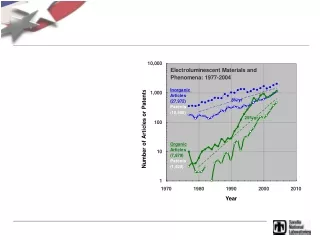
Journal article and patent counts by 4-year periods (e.g. 1977-80, 1981-84) for LEDs and OLEDs.
OLED dataset OLED dataset
A1 A1: GaAs, InP (22%) 43 23 22 13 17 10 15 28 33 46 47 38 B2: Quantum Wires/Dots (5%) 21 26 42 5 50 30 29 B1 B1: Carrier Dynamics (4%) Increasing electron and hole localization 8 A2 41 14 A5: S, Se (7%) 48 1 A2: Se, Te, Mn, Fe (11%) 6 20 A7: Si, SiO2 (9%) 24 A3 16 27 A3: GaN (10%) 36 3 3 40 40 C1 C1: HMVR Instrumentation (1%) A4 2 A4: ZnO (2%) 19 34 B2 A5 A6 C2: Sensors, Phototherapy, Optics (4%) 4 A7 7 44 49 37 32 35 9 9 12 18 18 39 39 C2 31 25 25 45 45 A6: Organics (23%) 11 11 Maps of the SSL scientific literature. Level-3 clusters with level-4 assignments and a stylized version of the level-4 map (inset). Sizes of clusters in the stylized map reflect relative numbers of papers in each cluster.
Performance and trends in the scientific literature by country in the 11 level-4 groupings.
A1: GaAs, InP B1: Carrier Dynamics Nanophosphors Nanowires Electro- phosphorescence A2: Se, Te, Mn, Fe A3: GaN Spintronics Polyfluorenes A5: S, Se C1: HMVR Instrumentation A7: Si, SiO2 A4: ZnO AlGaN UV LEDs B2: Quantum Wires/Dots A6: Organics C2: Sensors, Phototherapy, Optics Heat mapping according to: Actual citations / Expected citations LOW HIGH Ratio < 0.5 0.5 - 1.0 1.0 - 2.0 2.0 - 3.0 > 3.0 Distribution and impact of recent topics (level-2 clusters) on the stylized map of the SSL scientific literature. Sizes of clusters in the stylized map reflect relative numbers of papers in each cluster.
E3: Indicators, Scanners (8%) F2: Portable Lights (6%) E3 16 4 11 F1: Backlights, Panels, Phosphors (15%) 53 5 37 36 57 23 E4: Sensors (4%) 44 F2 21 39 48 E4 35 25 27 52 22 61 8 38 34 42 F3: Lamps, Controls (19%) 60 20 F1 13 29 15 59 30 28 10 7 F3 56 Chips to Systems to Apps 32 26 17 E2 62 51 49 E2: Switches, Indicators (5%) 43 12 D1: OLEDs (18%) 41 E1: Linear Arrays (5%) E1 55 D2: LEDs & Optics (11%) D2 46 31 2 50 18 40 1 45 6 58 D1 9 19 33 47 14 3 24 D3 D3: LEDs & Heterostructures (8%) 54 Organics Inorganics Maps of SSL patents. Level-3 clusters with level-4 assignments and a stylized version of the level-4 map (insert). Sizes of clusters in the stylized map reflect relative numbers of patents in each cluster.
Performance and trends in the patent literature by country in the 10 level-4 groupings.
LED retrofitting lamps Photocuring and phototherapy OLED encapsulation Multicolor OLEDs E4: Sensors E3: Indicators, Scanners F2: Portable Lights Active- matrix displays F3: Lamps, Controls Thermal transfer for OLED fabrication F1: Backlights, Panels, Phosphors E2: Switches, Indicators E1: Linear Arrays D2: LEDs & Optics D3: LEDs & Heterostructures D1: OLEDs Phosphor-converted LEDs Ornamental LED packages Ink-jet printed OLEDs Heat mapping according to: Actual citations / Expected citations Heat mapping according to: Actual citations / Expected citations LOW LOW HIGH HIGH Ratio Ratio < 0.5 < 0.5 0.5 - 1.0 0.5 - 1.0 1.0 - 2.0 1.0 - 2.0 2.0 - 3.0 2.0 - 3.0 > 3.0 > 3.0 Distribution and impact of recent topics (level-2 clusters) on the stylized map of the SSL patent literature. Sizes of clusters in the stylized map reflect relative numbers of patents in each cluster.
Age distribution of level-2 clusters for scientific literature and patents.
Boolean Search Phrase:SSL = S1 OR S2 OR S3 OR S4 OR S5 OR S6 OR S7 S1 S2 S3 semic* lum* electrolum* OR electrophos* layer* OR copolym* OR polym* OR organic OR diode* OR semi* “active layer” OR “active region” OR “clad layer” OR “cladding layer” OR “well layer” OR epit* OR hetero* OR “pn junction” OR “II-VI” OR “III-V” OR “III-nitride” OR “gallium nitride” OR “GaN” S4 copolym* OR polym* OR organic OR “II-VI” OR “III-V” OR “III-nitride” OR “gallium nitride” OR “GaN” light emi* dev* OR display* OR “element” OR “elements” OR lamp* OR panel* OR phosphor* “plasma” OR “noble gas” OR fluoresce* “EL” S7 S6 S5 “an” OR “HB” OR “white” OR “UV” OR “blue” OR “green” OR “amber” OR “red” array* OR dev* OR display* OR element* “semiconductor light source” OR (solid state light*) “LEDs” OR OLED* OR (“a LED” NOT (“led to” OR “led from”)) LED
Partitioning the Dataset by Materials SSLInorganic = SSL NOT Organic SSLOrganic = SSL AND Organic oled* OR polym* OR monom* O = OR ligand OR hydroxy OR macromol* OR (organic <not> metalorganic) SSL