I-Nanotechnology
Nanotechnolgy : Enabling Technology for Applications Laila H. Abuhassan Former Senator Professor of Physics & Nanotechnology Department of Physics/University of Jordan, Jordan Zarqa University, Zarqa , Jordan May 27, 2014. I-Nanotechnology.

I-Nanotechnology
E N D
Presentation Transcript
Nanotechnolgy: Enabling Technology for ApplicationsLaila H. AbuhassanFormer SenatorProfessor of Physics & Nanotechnology Department of Physics/University of Jordan, JordanZarqaUniversity, Zarqa, JordanMay 27, 2014
I-Nanotechnology Nobel Laureate physicist Richard Feynman in his famous 1959 lecture: "There's Plenty of Room at the Bottom" in which he first proposed that the properties of materials and devices at the nanometer range would present future opportunities. The term reached greater public awareness in 1986 with the publication of “Engines of Creation: The Coming Era of nanotechnology” by Eric Drexler.
NT : New Doors are Open and New Opportunities are Accessible • Small size corresponding to that of macro-molecules and comparable to that of basic biological structures. • Size-dependent properties • Chemical - reactivity, catalysis, unique bonding. • Thermal - melting temperature. • Mechanical - adhesion, capillary forces. • Electrical- tunneling. • Optical - absorption, scattering, and dominance of wave nature of light. • Magnetic - spintronics, superparamagnetic effect. • High surface to volume ratio • Unique environment of surface atoms. • Surface dominance over bulk and surface forces dominate over gravity. • Importance of quantum mechanical effects. • NEW KNOWLEDGEand PROPERTIESenableNEW APPLICATIONS.
Why Nanotechnology? • As the high technological industries (semiconductors, printing, storage ...etc) reach size limitations, they are turning to nanotechnology to further shrink and/or improve their products. • The promise of nanotechnology is based upon the ability to create nanostructured materials that will produce novel properties on the macroscale. • Nanotechnology is knowledge-based, in contrast to existing industries that are mainly resource-based.
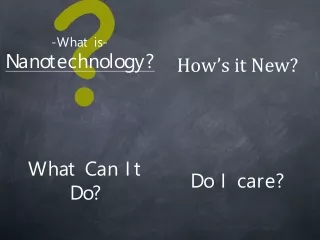
What is Nanotechnology? • I will introduce the Concept of Nanotechnology: • How miniaturization to produce nanostructures impacts the Fundamental Properties of Materials; • How one can reconstitute the nanostructures into Custom Materials for specific Applications; • I will mention specific ‘selected’ nanomaterials • (From my Lab): Properties & examples of possible applications in different fields;
Definition of Nanotechnology • Nanotechnology is the purposeful creation, manipulation and machining of engineered materials at the nanoscale. • Nanotechnology is a ‘revolution’ because it is changing in a fundamental way how we build things. It is reshaping the way technological products are made and the way they work.
Nanotechnology is the ability to measure, see, manipulate and manufacture things usually between 1 and 100 nanometers (nm).
Nanotechnology is Multidisciplinary - Physics - Chemistry - Materials Science - Informatics - Engineering - Life Sciences - Mathematics - Electronics - Optics - Imaging
The most urgent challenges facing the just beginning new century are focussing on the fields of: Health, Food and Energy Only Examples-Related to these Issues will be discussed.
How miniaturization impacts the fundamental properties of materials • When matter is manipulated on the near-atomic size range, optical, electrical, magnetic, and other properties of materials change. The physiochemical as well as magnetic, electrical and optical properties of the nanomaterial are very different from their bulk counterparts. The mechanisms behind these changes are not yet clearly understood. Despite this incomplete understanding, it is still possible to attribute the novel qualities of these nanomaterials to the following changes in internal structure:
Quantum mechanical effect: as the particle size approaches the atomic/molecular scale, discrete energies associated with electron orbits become more evident causing non-linear property effects. This will alter the electrical and optical properties of the nanomaterials, • The increased total surface area of grains, as grain size is decreased, will result in a change in the physical properties of the nanomaterials,
The increased volume of grain boundaries relative to unit structure, as grain size is decreased, will change the physical properties of the nanomaterials. • Besides, an increased chemical reactivity can be obtained by the large number of atoms on the surface of nanomaterials providing sites for reactions
Nanofabricaton or Processing of nanomaterials Two fundamental approaches: • ‘Top-down’ approach: involves reconstructing the bulk material in order to create nanostructures. Examples are: mechanical alloying, severe plastic deformation, and electrochemical etching techniques. • ‘Bottom-up’ approach: nanomaterials are constructed from the basic building blocks, such as atoms and molecules. Examples: inert gas condensation, and different coating techniques. Self-assembly is a ‘bottom-up’ process. • Hybrid - Combined Top down and Bottom up
In general, All Properties (electrical, optical, chemical, mechanical, thermal, magnetic, ..etc) of Nanomaterials are: • Very different from their bulk counterpart, • Technologically desirable/useful, • Exhibited on Macroscale, • Selectively controlled by engineering the size, morphology, and composition of Nanomaterial.
Reconstitution of nanostructures into custom materials I I- Incorporate the small particles into other materials, exploiting their unusual novel properties to create ‘composite materials’ with properties that are enhanced or entirely different from those of their parent materials. Examples: • Ceramic nanomaterial when mixed with a polymer, results in a nanocomposite that can have a combination of hardness and toughness never seen in the natural world.
Synthetic composite material that can automatically ‘heal itself’ when it is broken or cracked. This technology has the potential to double or triple the life span of bridges, planes, and other structures. Microelectronics industry may benefit from this self-healing technology. • Xerox, Kodak and others are replacing traditional toners with nano-sized particles that are bundled together into larger particles. These particles are more uniform in shape and color than conventional toners.
More Examples: • Stain-resistant fabrics, • IBM has demonstrated a device with a data storage density of a trillion bits per square inch, the equivalent of 25DVD’s on a surface the size of a postage stamp. • Seagate, hard drive manufacturer, announced a one-inch hard drive that you can throw against the wall and it continues to run very well. • Fuji Photo Film company uses extremely thin coatings and magnetic particles in its archival tapes.
Reconstitution into custom materials II II- Fabricate functional nano components that have specific predetermined characteristics. Examples: • Conducting carbon nanotubes for efficient power transmission. • Nano-sized probes for testing, localizing and may be treating diseases.
Specific Interesting Applicationsfrom fuel cells to surgical instruments • An excellent example of applying a base technology is liquid crystal polymer (LCP) electronics packaging. Gore and Kuraray (Japan) are selling LCP films for use as printed circuit board materials. LCPs are also beneficial as electronic substrates and packaging platforms, • fingernail sized electronic device having the capacity to store several gigabytes of data,
Nanotechnology-based sensors have the potential to replace the presently used traditional sensors, • Cleaning up polluted sites, • Monitoring water sources, • Corrosion-resistant optical selective coatings, • Advanced nanocomposite materials for optical selective absorber coatings,
Lab-on-a-chip diagnostic techniques, • Imaging agents that can identify cancer cells and treat them prior to their spreading, • Controlled and Targeted Drug Delivery Systems that can kill cancer cells while leaving the healthy tissue unharmed, • Artificial tissues that replace diseased organs and even repair nerve damage,
Creation of novel nanostructures that could serve as new kinds of drugs for treating cancer, Parkinson’s, and cardiovascular disease, • Supporters and possible replacements for noble metal catalysts for use in fuel cells and the paints and coatings industries, • ……….etc.
On the other hand: Issues of concern: “Biosafety and Toxicity”
I will present ‘as an example’ some recent results we have been conducting in collaboration with University of Illinois on: • - Preparation of Si & Ge nanomaterials, • - Application of the Si nanomaterial to Cancer Tissues, • - The Requirements for Collaborative Research work.
III-International Collaborative Research An Example Collaboration Team: University of Illinois, U.S.A. Sussex University, U.K. Yarmouk University, Jordan Faculty of Medicine (University of Jordan) Faculty of Pharmacy (University of Jordan) Biology Department (University of Jordan) Chemistry Department (University of Jordan)
Funded by: • University of Jordan • HCST • University of Illinois • US NSF
Reconstitution • Nanomaterial is extracted from the etched strips and kept as colloid in a solvent; • Reconstitution into thin films by: • - Evaporation • - Spin coating • - Electrodeposition
Results from collaboration on silicon with the University of Illinois • Preparation of silicon and germanium nanomaterials and nano components, • Characterization of the fabricated nanomaterials, • With enhanced support and furnishing of critical equipment, Technology Transfer can be successful, • There are future plans to engineer advanced nanomaterials, • Patents and impact, • Applications, • Publications
Recommendations Pooling resources Continuous funding Building collaborations internally and externally Formulation of national team in different disciplines: Physics, Chemistry, Molecular biology, Medicine, Agriculture, and Engineering.
Our work which started in 1992 has encouraged scientists to study the effect of nanomaterials in the different scientific disciplines and will contribute to the development of this Science/Technology in this region.
More work is being conducted at the University of Jordan and other Universities in Jordan. Examples of nanomaterials produced: • Copper, • Gold, • Magnetite, • Membranes, • And others……
Additional Nanotechnology-Enabled Solutions: Impacts on Solar Cells: Nanoparticles Improve efficiency & lifetime. Band gap of these nanoparticles depends upon their size.
Additional Impacts of Nanotechnology on Energy-Related challenges: • Lighting Technology • In Europe, about 10 percent of the electrical power produced is used for lighting.
Semiconducting Nanoparticles fluoresce, the colour depending only on the particle size. -LEDs (Light emitting Diodes): systems That convert electricity into light very efficiently. -LEDs need only 50% of the power Required by a normal bulb in order to produce same amount of light. LEDs are produced with the aid of Nanotechnology. • LEDs in traffic lights save service time and energy, • Quality brake lights,…
شكرا لحسن الإستماع ليلى أبو حسان