Instruction Counter
Register File. R1_en. Instruction Counter. R1. Address [3..0]. CLK. Arithmetic Logic Unit. R1_Sel. R1Out [3..0]. Reg_Clr. R2_en. Add. R2. Instruction ROM 0000: 000 0000 0001: 001 0001 0010: 010 0010 0011: 100 0000 0100: 011 0000. Inst [3..0]. R2Out [3..0].

Instruction Counter
E N D
Presentation Transcript
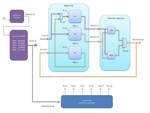
Register File R1_en Instruction Counter R1 Address [3..0] CLK Arithmetic Logic Unit R1_Sel R1Out [3..0] Reg_Clr R2_en Add R2 Instruction ROM 0000: 000 0000 0001: 001 0001 0010: 010 0010 0011: 100 0000 0100: 011 0000 Inst [3..0] R2Out [3..0] ALU Out [3..0] Inst [6..0] Reg_Clr R3_en R3 ALU_Out ALU_Sel Mult Reg_Clr R1_en R2_en R3_en R1_Sel Reg_Clr ALU_Sel Control Unit (Instruction Decoder) Instruction [6..4]
Register File R1_en ???? Instruction Counter R1 ???? Address [3..0] 0000 CLK Arithmetic Logic Unit R1_Sel R1Out [3..0] Reg_Clr ???? ???? R2_en Add R2 Instruction ROM 0000: 000 0000 0001: 001 0001 0010: 010 0010 0011: 100 0000 0100: 011 0000 Inst [3..0] ???? R2Out [3..0] ???? ALU Out [3..0] Inst [6..0] Reg_Clr R3_en ???? R3 ALU_Out ???? ALU_Sel Mult ???? Reg_Clr Clock cycle 0 Start! 0% through clock cycle Instruction Counter is initially at 0 and will output 0 (and increment its counter). Initially, control unit is outputting 0 for everything, so all the registers are not enabled, the muxes select input 0, and they are all being cleared. Note, the rest of the system is still outputting data, but right now it’s all “junk” because we have no idea what the values are, nor do we care. 0 0 0 0 0 0 R1_en R2_en R3_en R1_Sel Reg_Clr ALU_Sel Control Unit (Instruction Decoder) Instruction [6..4]
Register File R1_en 000 Instruction Counter R1 ???? Address [3..0] 0000 CLK Arithmetic Logic Unit R1_Sel R1Out [3..0] Reg_Clr ???? ???? R2_en Add R2 Instruction ROM 0000: 000 0000 0001: 001 0001 0010: 010 0010 0011: 100 0000 0100: 011 0000 Inst [3..0] 0000 R2Out [3..0] Inst [6..0] ???? ALU Out [3..0] 000 0000 Reg_Clr R3_en ???? R3 ALU_Out ???? ALU_Sel Mult ???? Reg_Clr Clock cycle 0 5% through clock cycle Instruction ROM will output the data at the address it is fed. Since it is fed 0000, it will output the first instruction. Control Unit receives the first 3 bits of the instruction to determine what to do. Register file ALSO gets the data, but since control unit was previously outputting 0 for everything, it doesn’t really matter since the register file is effectively turned off. 0 0 0 0 0 0 R1_en R2_en R3_en R1_Sel Reg_Clr ALU_Sel Control Unit (Instruction Decoder) Instruction [6..4]
Register File R1_en Instruction Counter 0000 R1 ???? Address [3..0] 0000 CLK Arithmetic Logic Unit R1_Sel R1Out [3..0] Reg_Clr ???? ???? R2_en Add R2 Instruction ROM 0000: 000 0000 0001: 001 0001 0010: 010 0010 0011: 100 0000 0100: 011 0000 Inst [3..0] 0000 R2Out [3..0] Inst [6..0] ???? ALU Out [3..0] 000 0000 Reg_Clr R3_en ???? R3 ALU_Out ???? ALU_Sel Mult ???? Reg_Clr Clock cycle 0 8% through clock cycle Control unit decodes the instruction and determines what to do by setting all the output pins accordingly. This is an init instruction, so the control unit will set Reg_Clr high to clear out our registers. This clears the register, and the registers ignore whatever is being sent into it. Our CPU is now stable, and it will remain this way until the next clock cycle. The registers will update on the next clock cycle, so it still currently outputs ????. 1 1 1 D 1 D R1_en R2_en R3_en R1_Sel Reg_Clr ALU_Sel Control Unit (Instruction Decoder) 000 Instruction [6..4]
Register File R1_en Instruction Counter 0000 R1 ???? Address [3..0] 0001 CLK Arithmetic Logic Unit R1_Sel R1Out [3..0] Reg_Clr 0000 ???? R2_en Add R2 Instruction ROM 0000: 000 0000 0001: 001 0001 0010: 010 0010 0011: 100 0000 0100: 011 0000 Inst [3..0] 0000 R2Out [3..0] Inst [6..0] 0000 ALU Out [3..0] 000 0000 Reg_Clr R3_en ???? R3 ALU_Out 0000 ALU_Sel Mult ???? Reg_Clr Clock cycle 1 0% through clock cycle Instruction counter now outputs a 0001 because the clock rising edge makes it increment. Registers are now outputting 000 as well, this happens as soon as the next clock cycle begins. 1 1 1 D 1 D R1_en R2_en R3_en R1_Sel Reg_Clr ALU_Sel Control Unit (Instruction Decoder) 000 Instruction [6..4]
Register File R1_en Instruction Counter 0000 R1 ???? Address [3..0] 0001 CLK Arithmetic Logic Unit R1_Sel R1Out [3..0] Reg_Clr 0000 ???? R2_en Add R2 Instruction ROM 0000: 000 0000 0001: 001 0001 0010: 010 0010 0011: 100 0000 0100: 011 0000 Inst [3..0] 0000 R2Out [3..0] Inst [6..0] 0000 ALU Out [3..0] 001 0001 Reg_Clr R3_en ???? R3 ALU_Out 0000 ALU_Sel Mult ???? Reg_Clr Clock cycle 1 5% through clock cycle Instruction ROM now will output the data stored in address 0001, which is 001 0001. Both adder and multiplier start to work on the new data now. 1 1 1 D 1 D R1_en R2_en R3_en R1_Sel Reg_Clr ALU_Sel Control Unit (Instruction Decoder) 000 Instruction [6..4]
Register File R1_en Instruction Counter R1 0001 Address [3..0] 0001 CLK Arithmetic Logic Unit R1_Sel R1Out [3..0] Reg_Clr 0000 ???? R2_en Add R2 Instruction ROM 0000: 000 0000 0001: 001 0001 0010: 010 0010 0011: 100 0000 0100: 011 0000 Inst [3..0] 0001 R2Out [3..0] Inst [6..0] 0000 ALU Out [3..0] 001 0001 Reg_Clr R3_en ???? R3 ALU_Out 000 ALU_Sel Mult ???? Reg_Clr Clock cycle 1 8% through clock cycle Control unit receives the new instruction and decodes it. Register file also gets the new data 0001. It is a move instruction into register 1, so control unit sets the control lines accordingly. Because of this, R1 will receive 0001 through the mux. R2 also receives 0001 but since R2_en is off, it will ignore that. But nothing happens until the next clock cycle. 1 0 0 0 0 D R1_en R2_en R3_en R1_Sel Reg_Clr ALU_Sel Control Unit (Instruction Decoder) 001 Instruction [6..4]
Register File R1_en Instruction Counter R1 0001 Address [3..0] 0001 CLK Arithmetic Logic Unit R1_Sel R1Out [3..0] Reg_Clr 0000 0000 R2_en Add R2 Instruction ROM 0000: 000 0000 0001: 001 0001 0010: 010 0010 0011: 100 0000 0100: 011 0000 Inst [3..0] 0001 R2Out [3..0] Inst [6..0] 0000 ALU Out [3..0] 001 0001 Reg_Clr R3_en ???? R3 ALU_Out 0000 ALU_Sel Mult ???? Reg_Clr Clock cycle 1 14% through clock cycle Adder finally finishes and calculates the proper value. 1 0 0 0 0 D R1_en R2_en R3_en R1_Sel Reg_Clr ALU_Sel Control Unit (Instruction Decoder) 001 Instruction [6..4]
Register File R1_en Instruction Counter R1 0001 Address [3..0] 0001 CLK Arithmetic Logic Unit R1_Sel R1Out [3..0] Reg_Clr 0000 0000 R2_en Add R2 Instruction ROM 0000: 000 0000 0001: 001 0001 0010: 010 0010 0011: 100 0000 0100: 011 0000 Inst [3..0] 0001 R2Out [3..0] Inst [6..0] 0000 ALU Out [3..0] 001 0001 Reg_Clr R3_en ???? R3 ALU_Out 0000 ALU_Sel Mult 0000 Reg_Clr Clock cycle 1 25% through clock cycle Multiplier finally finishes. Our ALU_Sel control line is a “don’t care” however so the ALU will be outputting either the adder or multiplier output. We don’t care which one though since R3_en is 0, so we won’t store it either way. The key point however is that the ALU still does its job every cycle regardless. The CPU is stable now, and will stay like this until the next clock cycle. 1 0 0 0 0 D R1_en R2_en R3_en R1_Sel Reg_Clr ALU_Sel Control Unit (Instruction Decoder) 001 Instruction [6..4]
Register File R1_en Instruction Counter R1 0001 Address [3..0] 0010 CLK Arithmetic Logic Unit R1_Sel R1Out [3..0] Reg_Clr 0001 0000 R2_en Add R2 Instruction ROM 0000: 000 0000 0001: 001 0001 0010: 010 0010 0011: 100 0000 0100: 011 0000 Inst [3..0] 0001 R2Out [3..0] Inst [6..0] 0000 ALU Out [3..0] 001 0001 Reg_Clr R3_en ???? R3 ALU_Out 0000 ALU_Sel Mult 0000 Reg_Clr Clock cycle 2 0% through clock cycle New clock cycle! Counter increments again, is now 2. The registers also will immediately output their new value too. 1 0 0 0 0 D R1_en R2_en R3_en R1_Sel Reg_Clr ALU_Sel Control Unit (Instruction Decoder) 001 Instruction [6..4]
Register File R1_en Instruction Counter R1 0001 Address [3..0] 0010 CLK Arithmetic Logic Unit R1_Sel R1Out [3..0] Reg_Clr 0001 0000 R2_en Add R2 Instruction ROM 0000: 000 0000 0001: 001 0001 0010: 010 0010 0011: 100 0000 0100: 011 0000 Inst [3..0] 0001 R2Out [3..0] Inst [6..0] 0000 ALU Out [3..0] 010 0010 Reg_Clr R3_en ???? R3 ALU_Out 0000 ALU_Sel Mult 0000 Reg_Clr Clock cycle 2 5% through clock cycle Instruction ROM will now output the instruction at address 0010, which is 010 0010. 1 0 0 0 0 D R1_en R2_en R3_en R1_Sel Reg_Clr ALU_Sel Control Unit (Instruction Decoder) 001 Instruction [6..4]
Register File R1_en Instruction Counter R1 0010 Address [3..0] 0010 CLK Arithmetic Logic Unit R1_Sel R1Out [3..0] Reg_Clr 0001 0000 R2_en Add R2 Instruction ROM 0000: 000 0000 0001: 001 0001 0010: 010 0010 0011: 100 0000 0100: 011 0000 Inst [3..0] 0010 R2Out [3..0] Inst [6..0] 0000 ALU Out [3..0] 010 0010 Reg_Clr R3_en ???? R3 ALU_Out 0000 ALU_Sel Mult 0000 Reg_Clr Clock cycle 2 7% through clock cycle Control unit decodes the new instruction, which is 010, which is a move into register 2. It will set the control lines. The register file also gets the new value and it will be fed the new value, but it won’t do anything until the next clock cycle. 0 1 0 D 0 D R1_en R2_en R3_en R1_Sel Reg_Clr ALU_Sel Control Unit (Instruction Decoder) 010 Instruction [6..4]
Register File R1_en Instruction Counter R1 ???? Address [3..0] 0010 CLK Arithmetic Logic Unit R1_Sel R1Out [3..0] Reg_Clr 0001 0001 R2_en Add R2 Instruction ROM 0000: 000 0000 0001: 001 0001 0010: 010 0010 0011: 100 0000 0100: 011 0000 0010 Inst [3..0] 0010 R2Out [3..0] Inst [6..0] 0000 ALU Out [3..0] 010 0010 Reg_Clr R3_en ???? R3 ALU_Out 0000 ALU_Sel Mult 0000 Reg_Clr Clock cycle 2 25% through clock cycle Adder and multiplier are finished, but once again the ALU out is a don’t care so we don’t know what is being output. R2_en is 1, so R2 will store 0010 at the rising edge of the clock cycle, and R1 and R2 will just ignore their input and keep their current values. Our system is stable and will wait like this until the next clock cycle. 0 1 0 D 0 D R1_en R2_en R3_en R1_Sel Reg_Clr ALU_Sel Control Unit (Instruction Decoder) 010 Instruction [6..4]
Register File R1_en Instruction Counter R1 ???? Address [3..0] 0011 CLK Arithmetic Logic Unit R1_Sel R1Out [3..0] Reg_Clr 0001 0001 R2_en Add R2 Instruction ROM 0000: 000 0000 0001: 001 0001 0010: 010 0010 0011: 100 0000 0100: 011 0000 Inst [3..0] 0010 R2Out [3..0] Inst [6..0] 0010 ALU Out [3..0] 010 0010 Reg_Clr R3_en ???? R3 ALU_Out 0000 ALU_Sel Mult 0000 Reg_Clr Clock cycle 3 0% through clock cycle New clock cycle. 0 1 0 D 0 D R1_en R2_en R3_en R1_Sel Reg_Clr ALU_Sel Control Unit (Instruction Decoder) 010 Instruction [6..4]
Register File R1_en Instruction Counter R1 ???? Address [3..0] 0011 CLK Arithmetic Logic Unit R1_Sel R1Out [3..0] Reg_Clr 0001 0001 R2_en Add R2 Instruction ROM 0000: 000 0000 0001: 001 0001 0010: 010 0010 0011: 100 0000 0100: 011 0000 Inst [3..0] 0000 R2Out [3..0] Inst [6..0] 0010 ALU Out [3..0] 100 0000 Reg_Clr R3_en ???? R3 ALU_Out 0000 ALU_Sel Mult 0000 Reg_Clr Clock cycle 3 15% through clock cycle Control unit decoded the instruction, which is an add of R1 and R2 and store in R3. It sets the proper control lines. 0 0 1 D 0 0 R1_en R2_en R3_en R1_Sel Reg_Clr ALU_Sel Control Unit (Instruction Decoder) 100 Instruction [6..4]
Register File R1_en Instruction Counter R1 ???? Address [3..0] 0011 CLK Arithmetic Logic Unit R1_Sel R1Out [3..0] Reg_Clr 0001 0011 R2_en Add R2 Instruction ROM 0000: 000 0000 0001: 001 0001 0010: 010 0010 0011: 100 0000 0100: 011 0000 Inst [3..0] 0000 R2Out [3..0] Inst [6..0] 0010 ALU Out [3..0] 100 0000 Reg_Clr R3_en 0011 R3 ALU_Out 0000 ALU_Sel Mult 0011 0010 Reg_Clr Clock cycle 3 25% through clock cycle Adder and multiplier are done. But ALU_Sel is set to 0 because we want the adder output, so that is what gets sent to R3. Our CPU is now stable and will wait until the next clock cycle. At the rising edge, R3 will store the ALU_Out value, which is 0011. 0 0 1 D 0 0 R1_en R2_en R3_en R1_Sel Reg_Clr ALU_Sel Control Unit (Instruction Decoder) 100 Instruction [6..4]
Register File R1_en Instruction Counter R1 ???? Address [3..0] 0100 CLK Arithmetic Logic Unit R1_Sel R1Out [3..0] Reg_Clr 0001 0011 R2_en Add R2 Instruction ROM 0000: 000 0000 0001: 001 0001 0010: 010 0010 0011: 100 0000 0100: 011 0000 Inst [3..0] 0000 R2Out [3..0] Inst [6..0] 0010 ALU Out [3..0] 100 0000 Reg_Clr R3_en 0011 R3 ALU_Out 0011 ALU_Sel Mult 0011 0010 Reg_Clr Clock cycle 4 0% through clock cycle Another new clock cycle! 0 0 1 D 0 0 R1_en R2_en R3_en R1_Sel Reg_Clr ALU_Sel Control Unit (Instruction Decoder) 100 Instruction [6..4]
Register File R1_en Instruction Counter R1 0011 Address [3..0] 0100 CLK Arithmetic Logic Unit R1_Sel R1Out [3..0] Reg_Clr 0001 0011 R2_en Add R2 Instruction ROM 0000: 000 0000 0001: 001 0001 0010: 010 0010 0011: 100 0000 0100: 011 0000 Inst [3..0] 0000 R2Out [3..0] Inst [6..0] 0010 ALU Out [3..0] 011 0000 Reg_Clr R3_en 0011 R3 ALU_Out 0011 ALU_Sel Mult 0011 0010 Reg_Clr Clock cycle 4 15% through clock cycle Instruction decoded, it is a move R3 into R1. So we set our control lines to enable R1, and to set R1_Sel to 1, which will select the R3 output. 1 0 0 1 0 D R1_en R2_en R3_en R1_Sel Reg_Clr ALU_Sel Control Unit (Instruction Decoder) 011 Instruction [6..4]
Register File R1_en Instruction Counter R1 0011 Address [3..0] 0100 CLK Arithmetic Logic Unit R1_Sel R1Out [3..0] Reg_Clr 0001 0011 R2_en Add R2 Instruction ROM 0000: 000 0000 0001: 001 0001 0010: 010 0010 0011: 100 0000 0100: 011 0000 Inst [3..0] 0000 R2Out [3..0] Inst [6..0] 0010 ALU Out [3..0] 011 0000 Reg_Clr R3_en ???? R3 ALU_Out 0011 ALU_Sel Mult 0010 Reg_Clr Clock cycle 4 25% through clock cycle Our adder and multiplier is done, but we don’t care what the outputs are. Our system is stable and will wait until the next clock cycle. At the rising edge, R1 will store 0011. The other registers will stay the same. 1 0 0 1 0 D R1_en R2_en R3_en R1_Sel Reg_Clr ALU_Sel Control Unit (Instruction Decoder) 011 Instruction [6..4]