Design and Implementation of a Stack-Based Calculator Using Dual-Port RAM and Finite State Machines
This project explores the design of a stack-based calculator utilizing digital logic principles, focusing on the implementation of a control unit defined by a finite state machine (FSM). The architecture includes dual-port RAM for efficient instruction and stack operations. Key components like the ALU, instruction register, and stack pointer are integrated to execute various arithmetic functions. The design also covers instruction encoding, data manipulation, and basic data flow techniques, making it a comprehensive exercise in computer system design and digital logic.

Design and Implementation of a Stack-Based Calculator Using Dual-Port RAM and Finite State Machines
E N D
Presentation Transcript
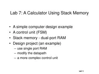
Lab 7: A Calculator Using Stack Memory • A simple computer design example • A control unit (FSM) • Stack memory - dual-port RAM • Design project (an example) • use single port RAM • modify the datapath • a more complex control unit
Motivation Computer Design as an application of digital logic design procedure Computer = Processing Unit + Memory System Processing Unit = Control + Datapath Control = Finite State Machine Inputs = Machine Instruction, Datapath Conditions Outputs = Register Transfer Control Signals Instruction Interpretation = Instruction Fetch, Decode, Execute Datapath = Functional Units + Registers Functional Units = ALU, Multipliers, Dividers, etc. Registers = Program Counter, Shifters, Storage Registers
Structure of a Computer Instruction Types Data Manipulation Add, Subtract, etc. Data Staging Load/Store data to/from memory Register-to-register move Control Conditional/unconditional branches subroutine call and return
A stack computer • stack: a last-in-first-out queue • operand registers: the top of the stack • simple instruction encoding • easy implementation • Instruction/data format • 9 bits • bit 8 = 1 • bit 7-0: operation code • bit 8 = 0 • bit 7-0: data (127~-127, two’s complement) • postfix format • 3, 5, 8, 6, - (3’H100), +, + (3’H101), EOF (3’H1FF)
Block Diagram and Basic Function • Basic components • dual-port RAM (stack) • one port for instruction access; the other for stack operation • IR, BREG, AREG, ALU Dual-port RAM stack inst. IR B A ALU
An example: 3, 5, 8, 6, -, +, + Dual-port RAM Dual-port RAM Dual-port RAM Dual-port RAM 3 6 5 8 5 8 B 3 A 3 5 A ALU ALU ALU ALU An example 3
Dual-port RAM Dual-port RAM Dual-port RAM Dual-port RAM + + EOF - 2 10 6 7 3 x 5 8 ALU ALU ALU ALU 3, 5 10 2 3 x 7
The block diagram Stack pointer Dual-port RAM stack inst. Program counter IR B A mux mux ALU
Dual-port RAM 16 * 9 bits inputs DI: data input WE: write_enable (active high) WCLK: synchronous RAM - positive-edge triggered A: primary port r/w address DPA: dual port read address outputs AO: primary port output DPO: dual port output primary port: stack access for data stack pointer: an up-down counter dual port: program access program counter: an up counter
Stack pointer push/write operation address = stack pointer ++ pop/read operation address = -- stack_pointer 4-bit up down counter input: ACLR, CLK, CLK_EN, UP_DWN_ output: CNTI: stack pointer CNTO: stack pointer for push stack pointer - 1 for pop possible problems longer propagation delay -1 + RAM access
Pipelining Fetch Exec Fetch Exec Fetch Exec Execution operation code execute the operation if available, pop data from the stack to A register (a memory read) data if A register contains data, push to the stack (a memory write) if B register contains data, shift to A register shift the data in IR to B register a dual-port memory is required one for fetching one for execution Operations
States S0 S1 one operand S2 two operands S3 >= two operands S4 >= three operands Error Halt Operations fetch shift push/pop execution OPR Fetch, sh_AB ,push FSM for the Control Unit
Inputs RESET: power-on reset IR: instruction register STP: stack pointer Outputs AB_SEL: select the inputs for registers A and B 0/1= push/pop A_CLK_EN, B_CLK_EN Latch regs A andB EOF_ = ~(IR == 1FF) ERROR_: syntax error IR_CLK_EN: latch IR STP_up_dn_: 0/1 = pop/push STP_CLK_EN: real push/pop Controls
Operations and Controls • fetch: IR_CLK_EN • shift: B_CLK_EN, (A_CLK_EN), !AB_SEL • push: STK_UP_DN_, STK_CLK_EN • pop: !STK_UP_DN_, STK_CLK_EN,A_CLK_EN • execution: AB_SEL, B_CLK_EN • halt: !HALT_
Final Design Check symbol info Add 7seg output to show result
Lab • Download an example project • The control-unit is incomplete • You can do timing verification • Perform timing verification • Answer a couple of questions • Design the control-unit • An FSM • Implement the calculator on the demo board • Display the result using the 7-seg LEDs
assign AO = q[A] ; assign DPO = q[DPA] ; always @(posedge WCLK or posedge RST) if (RST) begin q[0] = 9'h002 ; q[1] = 9'h003 ; q[2] = 9'h007 ; q[3] = 9'h002 ; q[4] = 9'h009 ; q[5] = 9'h100 ; q[6] = 9'h100 ; q[7] = 9'h101 ; q[8] = 9'h002 ; q[9] = 9'h008 ; q[10] = 9'h100 ; q[11] = 9'h100 ; q[12] = 9'h101 ; q[13] = 9'h1ff ; end else if (WE) q[A] = DI ; Dual Port RAM