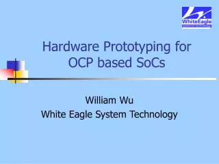
Hardware Prototyping for OCP based SoCs
190 likes | 402 Vues
Hardware Prototyping for OCP based SoCs. William Wu White Eagle System Technology. Content. SoC prototyping with FPGAs Why OCP based SoCs are good candidates for prototyping Challenges Example SoC Prototype on SwordFish System Prototyping Tips. SoC Prototyping with FPGAs.

Hardware Prototyping for OCP based SoCs
E N D
Presentation Transcript
Hardware Prototyping for OCP based SoCs William Wu White Eagle System Technology
Content • SoC prototyping with FPGAs • Why OCP based SoCs are good candidates for prototyping • Challenges • Example SoC Prototype on SwordFish System • Prototyping Tips
SoC Prototyping with FPGAs • Use one or more FPGA to emulate the function of a SoC to enable the validation of hardware, software and firmware on a single platform • Use of OCP for designing SoCs results in faster and less expensive prototyping
The Need for Prototyping • Verification • functional • system level • Early Software Development • System Development board verification • Did I mention software?
OCP Advantages for Prototyping • OCP and Sonics Backplane provide the following advantages: • Distributed Architecture for Bus Control • Upper Limit on the number of bus signals • Group the IP blocks and their bus interface modules together. • The RTL is partitioned into multiple FPGAs and the interface between FPGAs is the SoC Bus
Simple Partitioning SB signals on chip interconnect on chip interconnect
OCP makes prototyping easier • Easier to partition across multiple FPGAs • Easier to iterate design changes • Higher speeds up to 40 MHz with no strain
Prototyping Challenges • Design Partition • What to do with analog portion • IO interface • Clock scheme design
Design Partition • Where to draw the lines for SoC design? • Partition made easy with OCP based design
Analog PortionMixed-Signal Design • Separate the Analog portion • Construct the equivalent behavior with analog components • Put the analog components on the expansion card • Design wrapper RTL & circuit as necessary
IO Interface • Slow Speed IO is not a big problem • Strict timing interfaces are challenging • Divide the design to real world speed portion and prototyping speed portion • Use buffer for communication • Design Special interface circuit • Like Automatic Retry generation for PCI
IO Interface cont. • DDR memory interface • DQS used as read data clock source • FPGA doesn’t like to use data signal as clock source • Use the DCM to generate different phases of the source clock and use them as clock signals • FPGA supports SSTL2 IO standards • SSTL2 require Vref of 1.25V • Beware of bank limitation
Clock Scheme Design • Make good use of the DLL in FPGA: • Generate different divided clocks • Generate different phases • A system clock that goes to other FPGAs should have feedback path for skew minimization • Gated Clock • Use output mux to select flopped data and un-flopped data • Use clock enable pin on the FF • Synplicity Certify tool auto correct gated clock
Example OCP based SoC • SoC • Two processors • DDR SDRAM Controller • Two speeds of A/D and an D/A • 20 other IP blocks with various IO • 4 million gates • Over 300 MHz
SwordFish System • A SoC emulation system for OCP based designs • It is built using Xilinx Virtex II FPGAs • The SwordFish Software • The RTL-Slicer partitions the SoC RTL for each FPGA • The IO-Mapper allocates the RTL ports to physical IO pins • Platform Control & Monitor • The emulation runs in the 40MHz range
Example SoCChallenges • Results • Three Xilinx Virtex-II 8000 • Running at 30Mhz
Tips • Start early • Prototyping person/team should be closely involved in the design process • Integrated logic analyzer is your friend • Modular / incremental design flow reduces the turn around time
Summary • SoC prototyping with FPGAs is a powerful tool • OCP based SoCs are excellent candidates for prototyping • The challenges are easily identifiable and therefore solvable