Analog to Digital Converters
440 likes | 880 Vues
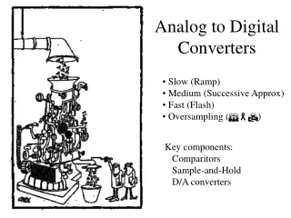
Analog to Digital Converters. Nyquist-Rate ADCs Flash ADCs Sub-Ranging ADCs Folding ADCs Pipelined ADCs Successive Approximation (Algorithmic) ADCs Integrating (serial) ADCs Oversampling ADCs Delta-Sigma based ADCs. Conversion Principles. ADC Architectures.

Analog to Digital Converters
E N D
Presentation Transcript
Analog to Digital Converters • Nyquist-Rate ADCs • Flash ADCs • Sub-Ranging ADCs • Folding ADCs • Pipelined ADCs • Successive Approximation (Algorithmic) ADCs • Integrating (serial) ADCs • Oversampling ADCs • Delta-Sigma based ADCs
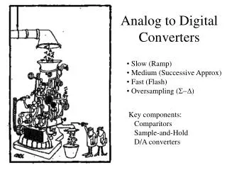
ADC Architectures • Flash ADCs: High speed, but large area and high power dissipation. Suitable for low-medium resolution (6-10 bit). • Sub-Ranging ADCs: Require exponentially fewer comparators than Flash ADCs. Hence, they consume less silicon area and less power. • Pipelined ADCs: Medium-high resolution with good speed. The trade-offs are latency and power. • Successive Approximation ADCs: Moderate speed with medium-high resolution (8-14 bit). Compact implementation. • Integrating ADCs or Ramp ADCs: Low speed but high resolution. Simple circuitry. • Delta-Sigma based ADCs: Moderate bandwidth due to oversampling, but very high resolution thanks to oversampling and noise shaping.
System Definitions • n-Bit ADC • Sinusoidal Input • Swing: ±1[V] • fmax= ½ fconv Performance Limitations 1 Thermal Noise Limitation Clock Jitter (Aperture) Limitation Normalized Noise Powers: fin=½fconv Limiting Condition: Maximum Resolution:
Performance Limitations 2 Displays Seismology Audio Sonar Wireless Communications Ultra Sound Video Selection of ADC Architecture is driven by Application
Parallel or Flash ADCs Conceptual Circuit
Sub-Ranging ADCs Half-Flash or Two-Step ADC
… 2n1 Sub-Ranges Folding ADCs Principle Configuration
Folding Processor Example: 2-Bit Folding Circuit (2n-1+1)Io for n-Bit 2Io
Successive Approx. ADCs Implementation Concept
DAC Realization 1 (Voltage Mode)
DAC Realization 2 Spread Reduction through R-2R Ladder
DAC Realization 3 Charge-Redistribution Circuit valid only during f2 • Pros • Insensitive w.r.t. Op-amp Gain • Offset (1/f Noise) compensated • Cons • Requires non-overlapping Clock • High Element Spread Area • Output requires S&H
DAC Realization 4 Spread Reduction through capacitive Voltage Division Example: 8-Bit ADC valid only during f2 Spread=2n/2
DAC Realization 5 Charge-Redistribution Circuit with Unity-Gain Amplifier Example: 8-Bit ADC Amplifier Input Cap. 16/15C Spread=½2n/2 Cp Gain Error: єG=-Cp/16C • Pros • Voltage divider reduces spread • Buffer low output impedance • No clock required • Cons • Parasitic cap causes gain error • High Op-amp common mode input required • No amplifier offset compensation
Sub-range Output (4 LSBs) Amplifier Output 0 0.5u 1u 1.5u 2u 2.5u 3u 3.5u 4u 4.5u 5u 5.5u 6u 6.5u 0 0.5u 1u 1.5u 2u 2.5u 3u 3.5u 4u 4.5u 5u 5.5u 6u 6.5u DAC8 with Unity-Gain Amplifier
DAC Realization 6 Current Mode Implementation
Current Cell & Floor Plan Symmetrical Current Cell Placement Array of 256 Cells Iout Current summingRail R Unit Current Cell Switching Devices Cascode Current Source
DAC Implementation Layout of 10-Bit Current-Mode DAC (0.5mm CMOS) Current summing Rails
Modified SA Algorithm 1 Idea: Replace DAC by an Accumulator Consecutively divide Ref by 2
Modified SA Algorithm 2 Idea: Maintain Comparator Reference (½ FS=Gnd) Double previous Accumulator Output First cycle only Accumulator
SC Implementation SC Implementation of modified SA ADC
Offset Compensated Circuit Offset Compensated SC Implementation
Building Blocks 1 Transconductance Amplifier
Building Blocks 2 Latched CMOS Comparator
Layout of 8-Bit ADC 165mm (0.5 mm CMOS)
Spice Simulation (Bsim3) 8-Bit ADC: fclk=10MHz fconv=1.25MHz
Pipelined ADCs Pipelined modified SA or Algorithmic ADC • Pros • Offset (1/f Noise) compensated • Minimum C-spread • One conversion every clock period • Cons • Matching errors digital correction for n>8 • Clock feed-through very critical • High amplifier slew rate required
Integrating or Serial ADCs Dual Slope ADC Concept Constant Ramp Prop. to Input Ramp • Using 2N/k samples requires Ref = FS/k • reduced Integrator Constant (Element Spread) N represents digital equivalent of analog Input
SC Dual-Slope ADC 10-Bit Dual-Slope ADC
Circuit Under Test Input Output Clock ADC Testing • Types of Tests • Static Testing • Dynamic Testing • In static testing, the input varies slowly to reveal the actual code transitions. Yields INL, DNL, Gain and Offset Error. • Dynamic testing shows the response of the circuit to rapidly changing signals. This reveals settling errors and other dynamic effects such as inter-modulation products, clock-feed-trough, etc.
Performance Metrics 1 Static Errors IDEAL ADC • Error Types • Offset • Gain • DNL • INL • Missing Codes
Amplitude fsig Performance Metrics 2 Frequency Domain Characterization Ideal n-Bit ADC: SNR = 6.02 x n + 1.76 [dB]
ADC Error Sources Static Errors • Element or Ratio Mismatches • Finite Op-amp Gain • Op-amp & Comparator Offsets • Deviations of Reference Dynamic Errors • Finite (Amplifier) Bandwidth • Op-amp & Comparator Slew Rate • Clock Feed-through • Noise (Resistors, Op-amps, switched Capacitors) • Intermodulation Products (Signal and Clock)
Static Testing • Servo-loop Technique • Comparator, integrator, and ADC under test are in negative feedback loop to determine the analog signal level required for every digital code transition. • Integrator output represents equivalent analog value of digital output. • Transition values are used to generate input/output characteristic of ADC, which reveals static errors like Offset, Gain, DNL and INL.
Dynamic Testing Test Set-up • Types of Dynamic Tests • Histogram or Code-Density Test • FFT Test • Sine Fitting Test
Histogram or Code-Density Test • DNL appears as deviation of bin height from ideal value. • Integral nonlinearity (INL) is cumulative sum (integral) of DNL. • Offset is manifested by a horizontal shift of curve. • Gain error shows as horizontal compression or decompression of curve.
Histogram Test • Pros and Cons of Histogram Test • Histogram test provides information on each code transition. • DNL errors may be concealed due to random noise in circuit. • Input frequency must be selected carefully to avoid missing codes (fclk/fin must be non-integer ratio). • Input Swing is critical (cover full range) • Requires a large number of conversions (o 2n x 1,000).
Simulated Histogram Test 8-Bit SA ADC with 0.5% Ratio Error and 5mV/V Comparator Offset
FFT Test Pros and Cons of FFT Test • Offers quantitative Information on output Noise, Signal-to-Noise Ratio (SNR), Spurious Free Dynamic Range (SFDR) and Harmonic Distortion (SNDR). • FFT test requires fewer conversions than histogram test. • Complete characterization requires multiple tests with various input frequencies. • Does not reveal actual code conversions
Simulated FFT Test 8-Bit SA ADC with 0.5% Ratio Error and 5mV/V Comparator Offset SNDR=49 dB ENOB=7.85 SFDR=60 dB