HCS12 Overview
HCS12 Overview. 8 & 16-Bit Microcontroller Division. Main Features :. • 16-bit HCS12 CPU – Upward compatible with HC11/ 12 instruction set – Interrupt stacking and programmer’s model identical to HC11/ 12 – 20-bit ALU – Instruction pipe

HCS12 Overview
E N D
Presentation Transcript
HCS12 Overview 8 & 16-Bit Microcontroller Division
Main Features: • 16-bit HCS12 CPU – Upward compatible with HC11/ 12 instruction set – Interrupt stacking and programmer’s model identical to HC11/ 12 – 20-bit ALU – Instruction pipe – Enhanced indexed addressing • SIM (System integration module) – MEBI (Multiplexed External Bus Interface) – MMC (Module Mapping Control) – INT (Interrupt control) – BKP (Breakpoints) – BDM (Background Debug Mode) • Clocks and Reset Generator (CRG) - low current oscillator, PLL, reset, clocks, COP watchdog, Real time interrupt, clock monitoring • Memory – Split Gate Flash EEPROM (paged) – Split Gate EEPROM (word write, 2 word erase) – zero wait state RAM • Peripherals – Enhanced Serial Communications Interface (SCI) – Serial Peripheral interface (SPI) – 1M bit per second, CAN 2.0 A, B msCAN module (with paged message buffers) – Universal Serial Bus 2.0 (USB) interface – Byte Data Link Controller (BDLC) – Inter-IC Bus (IIC) – 10-bit Analog-to-Digital Converter – Standard 8 channel Timer – Enhanced Capture Timer (ECT) – PWM module – Stepper Motor controller – LCD controller and more on the way! • On-chip Voltage Regulator – 2.25 to 2.75V Digital Supply Voltage generated using an internal Voltage Regulator – 4.75V to 5.25V Analog and I/O Supply Voltage • Technology: 0.25 micron CMOS – 50 MHz CPU equivalent to 25MHz bus operation (66/33MHz in design)
HCS12 Building Blocks • HCS12 CPU Core & System Integration Module • Support Modules: Vreg & Clocks and Reset Generator • Memories: Flash, RAM, EEPROM • Peripherals: Comms interfaces, ATD, Timer, etc. SCI 1 PWM 8 CHAN ECT 8 CHAN SCI 0 4K BYTES EEPROM 12K SRAM 256K FLASEEPROM Internal Bus CRG SPI 2 or PWM CH 4-7 SPI 1 or PWM CH 0-3 SPI 0 BKP INT MMI HCS12 CPU SIM CM BDM MEBI PLL PIT ms CAN 4 or IIC ms CAN 3 ms CAN 2 ms CAN 1 ms CAN 0 or BDLC PIM VREG ATD 1 ATD 0
HCS12 Documentation Device User Guide MC9S12DP256 Device User Guide (9S12DP256UG/D) [1Mb] HCS12 V1.5 Core User Guide (S12CPU15UG/D) [6Mb] Block User Guides PIM_9DP256 Block User Guide (9S12DP256PIMUG/D) FTS256K Block User Guide (S12FTS256KUG/D) EETS4K Block User Guide (S12EETS4KUG/D) CRG Block User Guide (S12CRGUG/D) ECT_16B8C Block User Guide (S12ECT16B8CUG/D) ATD_10B16C Block User Guide (S12ATD10B16CUG/D) [6Mb] SCI Block User Guide (S12SCIUG/D) SPI Block User Guide (S12SPIUG/D) PWM_8B8C Block User Guide (S12PWM8B8CUG/D) MSCAN Block User Guide (S12MSCANUG/D) VREG Block User Guide (S12VREGUG/D) Watch out for the Rev Number of each Guide - there is a list in the Device User Guide of which rev was appropriate when the device was created. Click here to learn how to receive up-to-date technical documentation Useful Engineering Bulletins EB386 HCS12 D-Family Compatibility Considerations EB376 A comparison of the MC9S12DP256 (mask set 0K36N) versus the HC12
Core Features (1 of 2) • HCS12 has identical programmers model to M68HC11/M68HC12 • No new registers • No changes in interrupt stacking order • Muxed and non-muxed external interfaces • Possible to reuse existing software source code • Note: timing loops change due to new clock frequency, • Byte counts and instruction cycle times. • Almost all peripheral drivers will require updating • Performance improvement when using new instructions • Reduced interrupt latency • Increased math speed • Increased performance • Instruction Queue data to increase performance • Instructions execute faster while remaining deterministic
Core Features (2 of 2) • HC11 instruction set with extra instructions designed with compilers in mind: • New instructions and addressing modes to support high level languages.* • Added • Stack pointer and program counter offset indexed addressing • 11 math instructions • Long branch instruction (16 bit offset) • Move instruction (memory to memory) • Min / max functions • Bit manipulations for entire memory map • Exchange / transfer • Table look-up and interpolate function • Looping construct • Fuzzy logic instructions * MC68HC12 and HCS12 have Identical Instruction Set.
HC05 / HC08 / HCS12 HC08 / HCS12 HCS12 Programmers Model 68HC11 = 68HC12 = HCS12 Programmers Model 8-Bit Accumulators A and B 7 A 0 7 B 0 or 16-Bit Double Accumulator D 15 D 0 Index Register X 15 X 0 Index Register Y 15 Y 0 Stack Pointer 15 SP 0 Program Counter 15 PC 0 5 PPAGE * 0 7 0 Condition Codes Register • Source code compatible • Identical stack frame • * PPAGE used by CALL & Return To Call (RTC). (paged HC(S)12 only) S X H I N Z V C Carry/Borrow (From MSB) Overflow Zero Negative (MSB = 1) I-Interrupt Mask Half Carry (For BCD) X-Interrupt Mask STOP Disable
Condition Code Register S X H I N Z V C MASKING BITS ARITHMETIC BITS • Reflect results of instruction execution. C - Carry/Borrow from MSB S - Disables STOP instruction when set. unsigned arithmetic X - Masks XIRQ request when set. V - 2's complement overflow indication - set by hardware reset, cleared by software. signed arithmetic - set by unmaskable XIRQ Z - Zero result I - Masks interrupt request from all IRQ level sources ( both external and internal ) N - Negative ( follows MS Bit of result ) when set. - set by unmasked I level request H - Half Carry from bit 3 to bit 4 or unmasked XIRQ ADD operations only
HCS12 Serial Interface Features • 2 SCI Interfaces • Up to 3 SPI interfaces • SCI is Asynchronous Communication Port • 13-bit break support • SPI is a Synchronous High Speed Communication Port • Modular Architecture allows future expansion • SCI & SPI are similar to MC68HC11 with enhancements • pins may be configured as general purpose I/O • Loop mode operation for debugging • SCI & SPI have single-wire function RxD0 TxD0 RxD TxD RxD TxD MISO MOSI SCK SS MISO MOSI SCK SS MISO MOSI SCK SS SCI0 P O R T S D D R S RxD0 TxD0 SCI1 MISO MOSI SCK SS SPI0 MISO MOSI SCK SS SPI1 MISO MOSI SCK SS SPI2
MC9S12 Enhanced Capture Timer • 16-bit main timer with 7-bit Prescaler • 8 IC/OC channels, 4 IC channels buffered • 16-Bit modulus Down-Counter with 4-bit prescaler for: • periodic interrupt time base • control IC/PA register latch • 4 8-Bit or 2 16-bit pulse accumulators with 4 8-bit buffer registers • independent Interrupt sources: 8 IC/OC, Timer OF, 3 PA, MC • 4 inputs with selectable Delay Counters to filter out spurious signals Control Bits load Register Bus Clock 16-Bit Modulo Down-Counter 16-Bit Free-running Main Timer Prescaler Prescaler Reset 0 COMPARATOR Pin Logic Delay Counter CAP./COM. Register Pulse Accumulator CH1 Hold Register Hold Register
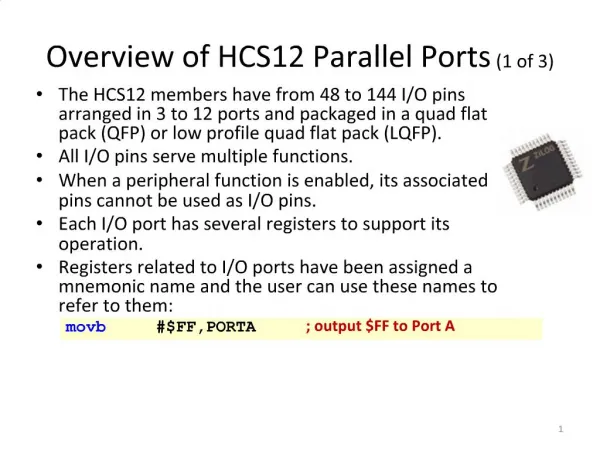
IOC0 PT0 PH0 IOC1 PT1 PH1 IOC2 PT2 PH2 Interrupt Logic IOC3 PT3 Timer PortT PortH PH3 IOC4 PT4 PH4 IOC5 PT5 PH5 IOC6 PT6 PH6 IOC7 PT7 PH7 PW0 PP0 PW1 PP1 PW2 PP2 PWM PW3 PP3 PortP PW4 PP4 PW5 PP5 PW6 PP6 PW7 PP7 RxD PS0 RxCAN SCI0 TxD PS1 TxCAN RxD PS2 RxCAN SCI1 TxD PS3 PortM PortS TxCAN SDI/MISO PS4 SDO/MOSI PS5 SCK PS6 SPI SS PS7 New: Port Integration Module PIM Standardized interface between peripheral modules and I/O pads for all ports except A,B,E,K. Port control function within standard peripheral modules has been removed • Standard Port features: • User Defined "electrical" characteristics on a pin by pin basis: • – reduced drive • – wired-or mode • – pull-ups /downs* • (* Here certain precautions are taken such as if the CAN • is enabled pull-up is allowed but pull-down is blocked) • -> High Flexibility • Port registers relocatable in • memory map -> High Flexibility PIM o Inter.L. PJ0 PJ1 PortJ SDA PJ6 IIC SDL PJ7 RxCAN CAN4 TxCAN RxB BDLC TxB PM0 CAN0 PM1 PM2 CAN1 PM3 RxCAN PM4 CAN2 PM5 TxCAN PM6 RxCAN CAN3 PM7 TxCAN
IIC Features • • Compatible with I2C Bus standard • • Multi-master operation • • Software programmable for one of 256 different serial clock frequencies • • Software selectable acknowledge bit • • Interrupt driven byte-by-byte data transfer • • Arbitration lost interrupt with automatic mode switching from • master to slave • • Calling address identification interrupt • • Start and stop signal generation/detection • • Repeated start signal generation • • Acknowledge bit generation/detection • • Bus busy detection • Low power modes support • Shared with msCAN 4
msCAN Bus • Up to 5 msCAN Modules (msCAN) • 3 Tx message buffers each Automatically Mapped • 5 Background Rx Buffers • Programmable I/O modes • Maskable interrupts • Programmable loop-back for self test operation • Independent of the transmission medium (external transceiver is assumed) • Open network architecture • Multimaster concept • High immunity to EMI • Short latency time for high-priority messages • Low power sleep mode, with programmable wake up on bus activity Note: msCAN 0 is multiplexed with BDLC msCAN 4 is multiplexed with IIC.
BDLC CONTROLLER (J1850) • SAE J1850 Compatible • 10.4Kbps VPW bit format • Digital noise filter • Collision detection • Hardware CRC generation & checking • Receive and Transmit Block mode supported • Supports 4X receive mode (41.6 Kbps) • Digital loopback mode • In-frame Response (IFR) Types 0, 1, 2, and • 3 supported • Power-Saving Stop and Wait modes with Automatic • Wakeup on Network Activity • Interrupt Generation with Vector Lookup Table
Analog to Digital Converter • 8/10 Bit Resolution. • 7 usec, 10-Bit Single Conversion Time. • Sample Buffer Amplifier. • Programmable Sample Time. • Left/Right Justified, Signed/Unsigned Result Data. • External Trigger Control. • Conversion Completion Interrupt Generation. • Analog Input Multiplexer for 8 Analog Input Channels. • Analog/Digital Input Pin Multiplexing. • 1 to 8 Conversion Sequence Lengths. • Continuous Conversion Mode. • Multiple Channel Scans.
PWM FEATURES - 8 INDEPENDENT PWM CHANNELS WITH PROGRAMMABLE PERIOD AND DUTY CYCLE. - 8-BIT 8-CHANNELS OR 16-BIT 4-CHANNELS. - DEDICATED COUNTER FOR EACH CHANNEL. - FLEXIBLE CLOCK GENERATION ( A, B, SA AND SB ) THAT COVERS WIDE RANGE OF FREQUENCIES. - PERIOD AND DUTY CYCLE ARE DOUBLE BUFFERED. - ALLOWS FOR IMMEDIATE PWM UPDATE. - POLARITY IS SOFTWARE SELECTABLE. - PROGRAMMABLE CENTER OR LEFT-ALIGNED PWM OUTPUT. - EMERGENCY SHUT DOWN
HCS12 Device Identification The part ID is located in two 8-bit registers PARTIDH and PARTIDL. The read-only value is a unique part ID for each revision of the die. The coding is as follows: Bit 15-12: Major family identifier Bit 11-8: Minor family identifier Bit 7-4: Major mask set revision number including FAB transfers Bit 3-0: Minor - non full - mask set revision The device memory sizes are located in two 8-bit registers MEMSIZ0 and MEMSIZ1.
MC9S12 Clocks & Reset Gen (CRG) • Crystal oscillator (OSC) • Colpitts with translated GND (as per HC12D- Family) or traditional Pierce configurations • Crystal Monitor (CM) • same as on HC12D-Family • Clock Quality Checker (CQC) • ensures valid clock for operation • Phase Locked Loop (PLL) • same as on HC12D-Family • Self Clock Mode with internal oscillator • System Clocks Generator (CGEN) • simplified clock chain: • Core clock = PLLCLK or OSCCLK • Peripherals clock = PLLCLK/2 or OSCCLK/2 (25% duty) • ECLK = PLLCLK/2 or OSCCLK/2 (50% duty) • no Slow Mode Clock • System Reset Generator (RGEN) • same Reset functionality as on HC12D-Family: • Reset by POR, COP, ext. Reset, Clock Monitor • Real Time Interrupt (RTI) - slightly different divider chain • Watchdog (COP) - slightly different divider chain • LOW POWER OSCILLATOR • SUPPORTS OPERATION UP TO 33 MHz CRG CQC OSC PLL EXTAL XTAL CM RTI VDDPLL XFC COP CGEN VSSPLL POR RGEN RESET Registers&Control Internal BusInterface
MC9S12 Low Power Modes: • Power Saving Design Features: • Low power Oscillator design (Engineered to avoid power-wasting harmonics) • User Configurable Low Power Peripheral modes • RUN Mode (full operation): • 65 mA max - However peripherals automatically shut down if not in use • WAIT Mode (CPU sleeping): • Peripheral modules can be configured in power conservation mode • 40 mA max with all modules enabled • 5 mA max with only Real Time interrupt enabled • STOP Mode (All modules stopped - Osc etc): • 30uA * Typical • Pseudo STOP Mode (All modules stopped): • 350uA * Typ - However Osc runs in low power mode enabling wake-up as fast as in WAIT mode • *At 27oC.
HCS12 Resets • POR (power-on reset) • Special delayed reset to allow oscillator to stabilize. Does not replace LVI function. • Thresholds: Releases when Vdd2.5 goes above 2.07V, Active when Vdd2.5 goes below 0.97V. • Clock quality check window is 50K self-clock cycles • If oscillatoramplitude and freq. are sufficient for 4096 cycles to be detected during a quality check window reset is exited using the XTALclock. • Up to 50 quality check windows can occur if oscillatoris slow to start. After 50 unsuccessful cycles Self Clock Mode is entered. • POR bit can be checked for cause of last reset. • POR bit can only be cleared by software.
MC9S12 - System Integrity... • Crystal Monitor Function: • Detects crystal failure and takes user-specified action - bad clock detect. • Clock Quality Checker: • Performs a window check on the oscillator to ensure that the MCU only executes from a stable clock - good clock detect. • Self Clock Mode: • Limited operation still possible even with temporary crystal problem • allows controlled shut-down in event of oscillator failure • allows for slow start-up of crystal oscillators • Flexible Watchdog: • Can be used as “windowed w/dog” - (eg refresh only between 75-100% of period) • - further reduces possibility of code run-away • Independent from PLL (clocked directly from crystal) - secure even if PLL fails • Further Reading: • AN2201/D: “ Low Battery Cranking Pulse in Automotive Applications” • (This app note shows how the HCS12 and SBC devices can be used together in a cost efficient manner for Automotive conditions).
BDM Development Tools BDM on MC9S12: • Low cost serial real-time emulation and debug • Single step, Run, or Trace the application code • On-chip hardware for multiple breakpoints • Replaces expensive emulator or bus analyzer • Works at full operating voltage and frequency range • Non-intrusive - no cumbersome emulator cables • In-circuit FLASH programming
MC9S12 0.25u Flash - the Best in the Industry: • Highly Flexible Flash: • 5 volt FLASH - no external charge pump required • Market-leading Flash Granularity - 512B Flash Erase / 2B Program • - Virtual EEPROM implementation possible for EE extension • 4 independently programmable Flash Segments • - Can erase one block whilst reading another • High Speed Programming: • Fast Flash Page Erase - 20ms (512bytes) • Can program 16 bits in 20us • Total Program Time for 128K Code down to:<5 seconds! • (App note AN2204 "Fast NVM Programming for the MC9S12DP256" is now published) • Efficient End Of Line Programming Possible
HCS12 Power Supplies • Vddr: Supplies regulator and Ports A,B,E,H - connect to 5V and bypass with 100 nF • Vdd1,2: Outputs from 2.5V regulator. Supply core - bypass with 47-220 nF depending upon EMC results. • Vddpll: Output from 2.5V regulator. Supplies Osc. and PLL - bypass with 22-100 nF • Vdda: Supply to A/D. Connect to 5V and bypass with 22-100 nF • Vrh: Reference for A/D. Connect to 5V and bypass with 10 nF • Vddx: Supply for all ports except those supplied by Vddr. Connect to 5V and bypass with 47-220 nF. Add 10 uF if big loads are switched.
Technical Subscription Service Make sure you have the most up-to-date technical documentation on all Motorola semiconductor products. Subscribe to receive weekly e-mail updates about new and revised technical documentation for Motorola products. Each e-mail will contain direct links to the new documentation and the product home page. Visit Motorola's Semiconductor Products Sector Web site, and select "products" from the Product Catalog, Design Resources, Communications, Networking or Automotive sections. Signing up is as easy as one, two, three: 1. Select a category of products. 2. Select the product of your choice. 3. Once on the product page, select the link titled "Subscribe for Updates" on the right side of the page. You may unsubscribe from this service at any time by following the instructions at the bottom of the update e-mail or by changing your subscription preferences after logging in. Why wait? Sign up today!