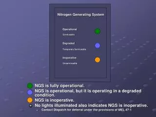
Download
1 / 49
540 likes | 850 Vues
Chapter 8 The Operational Amplifier (Part I) ~ Using PSpice. The Ideal Op Amp Noninverting Ideal Op Amp Op Amp Giving Voltage Difference Output Frequency Response of the Op Amp Using a Subcricuit for the Op Amp Op Amp differentiator Circuit Op Amp Integrator Circuit

E N D
Chapter 8 The Operational Amplifier (Part I) ~ Using PSpice • The Ideal Op Amp • Noninverting Ideal Op Amp • Op Amp Giving Voltage Difference Output • Frequency Response of the Op Amp • Using a Subcricuit for the Op Amp • Op Amp differentiator Circuit • Op Amp Integrator Circuit • Response to Unit Step Function • Double Op Amp Circuit
The Ideal Op Amp • High input resistance, zero output resistance, and high voltage gain
The Ideal Inverting Op Amp Negative feedback connection PSpice version of the circuit
Input File Ideal Operational Amplifier VS 1 0 1V E 3 0 0 2 200E3 RI 2 0 1G R1 1 2 1K R2 3 2 10K .OP .OPT nopage .TF V(3) VS .END
Run the Analysis and Verify • Run V(3)/VS=-9.999 • Verify Vo/Vs=-R2/R1=-10K/1K=-10
Noninverting Ideal Op Amp Noninverting ideal op amp Noninverting ideal op amp model
Input File Ideal Operational Amplifier, Noninverting VS 1 0 1V E 3 0 1 2 200E3 RI 1 2 1G R1 2 0 1k R2 3 2 9k .op .opt nopage .TF V(3) VS .END
Run and Verify • V(3)/VS=10, • Vo/Vs=1+R2/R1=1+9K/1K=10
Input File Op Amp Giving Voltage Difference Output VA 1 0 3V VB 4 0 10V E 5 0 3 2 200E3 RI 2 3 1G R1 1 2 5k R2 5 2 10k R3 4 3 5k R4 3 0 10k .OP .OPT nopage .TF V(5) VB .END
Run and Verify • Verify that Vo=R2(Vb-Va)/R1=10k(10v-3v)/5k=14v • V(5)=14V
Frequency Response of the Op Amp • Model for the frequency response of an op amp fc=10Hz
Input File Op Amp Model with 3-dB frequency at 10 Hz for Open-Loop Gain VS 2 0 AC 1mV EG 3 0 2 1 1E5 E 6 0 4 0 1 RI1 3 4 1k RO 6 5 50 R1 0 1 10k RL 5 0 22k RIN 1 2 1MEG C 4 0 15.92uF .AC DEC 40 1 1MEG .PROBE .END
Modify Input File Op Amp Model with 3-dB frequency at 10 Hz for Open-Loop Gain VS 2 0 AC 1mV EG 3 0 2 1 1E5 E 6 0 4 0 1 RI1 3 4 1k RO 6 5 50 R1 0 1 10k R2 5 1 240k RL 5 0 22k RIN 1 2 1MEG C 4 0 15.92uF .AC DEC 40 1 1MEG .PROBE .END
Using a Subcircuit for the Op Amp .subckt opamp m p vo eg a 0 p m 1e5 e c 0 b 0 1 rin m p 1meg ril a b 1k c b 0 15.92uF rol c vo 50 .ends
Op Amp Analysis Using Subcircuit Op Amp Analysis Using Subcircuit VS 2 0 AC 1mV R1 1 0 10k R2 3 1 240k X 1 2 3 opamp .AC DEC 40 100 1MEG .PROBE .subckt opamp m p vo eg a 0 p m 1e5 e c 0 b 0 1 rin m p 1meg ril a b 1k c b 0 15.92uF rol c vo 50 .ends .END
Op Amp Differentiator Circuit • Vo=-dv/dt
Input File Differentiator Circuit V 1 0 PWL (0, 0 1s, 1V 2s, 0) C 1 2 2F R 2 3 0.5 X 2 0 3 iop .subckt iop m p vo ri m p 1meg e vo 0 p m 2e5 .ends .TRAN 0.05s 2s .PROBE .END
Run and View Outputs V(1) Vo
Input File Integrator Circuit V 1 0 PWL (0 0 0.01ms, -1V 1s, -1V 1000.01ms, 0V 2s, 0V 2000.01ms, 1V 3s, 1V) R 1 2 0.5 C 2 3 2 X 2 0 3 iop .subckt iop m p vo ri m p 1meg e vo 0 p m 2e5 .ends .TRAN 0.05s 3s .PROBE .END
Run and View Output V(1) Vo
Response to Unit Step Function • By definition, it remains at zero volts until t=0, and from that time forward it is 1V.
Input File Response to Unit Step Function Vs 1 0 PWL (0, 0 1us, 1v 5s, 1v) C 2 3 0.125 R 2 3 2 R1 2 0 1 X 2 1 3 iop .subckt iop m p vo ri m p 1meg e vo 0 p m 2e5 .ends .TRAN 0.05s 3s .PROBE .END Vo(t)=(3-2e-4t)u(t)
Input File Double Op Amp Circuit for Gain-Bandwidth Analysis VS1 2 0 AC 1mV R1 1 0 10k R2 3 1 240k X1 1 2 3 opamp VS2 5 0 AC 1mV R3 4 0 10k R4 6 4 15k X2 4 5 6 OPAMP .AC DEC 40 100 10MEG .PROBE .subckt opamp m p vo eg a 0 p m 1e5 e c 0 b 0 1 rin m p 1meg ril a b 1k c b 0 15.92uF rol c vo 50 .ends .END
Run and View Outputs OP Amp 1 OP Amp 2
Chapter 8 The Operational Amplifier (Part II) ~ Using Capture • Noninverting Ideal Op Amp • Op Amp for Voltage-Difference Output • Frequency Response of the Op Amp • Frequency Response of the uA741 • The uA741 as a Level Detector
Noninverting Ideal Op Amp Ideal op amp in Capture Ideal op amp
Run and View Output 20*log10(V(5)/V(2))
Run and View Output Frequency response of the uA741
V1 (VPWL) Settings (0v, 0s), (3v, 0.2s), (5v, 0.4s), (-5v, 0.6s), (-3v, 0.8v), (0v, 1s)
Run and View Output V(1) input V(5) Output