Chapter Outline
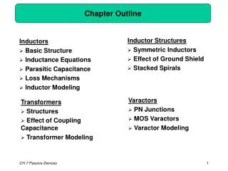
Chapter Outline. Inductor Structures Symmetric Inductors Effect of Ground Shield Stacked Spirals. Inductors Basic Structure Inductance Equations Parasitic Capacitance Loss Mechanisms Inductor Modeling. Varactors PN Junctions MOS Varactors Varactor Modeling. Transformers

Chapter Outline
E N D
Presentation Transcript
Chapter Outline Inductor Structures • Symmetric Inductors • Effect of Ground Shield • Stacked Spirals Inductors • Basic Structure • Inductance Equations • Parasitic Capacitance • Loss Mechanisms • Inductor Modeling Varactors • PN Junctions • MOS Varactors • Varactor Modeling Transformers • Structures • Effect of Coupling Capacitance • Transformer Modeling CH 7 Passive Devices 1
Motivation for On-Chip Integrated Inductors Reduction of off chip components ---> Reduction of system cost. Modeling issues of off-chip inductors The bond wires and package pins connecting chip to outside world may experience significant coupling CH 7 Passive Devices 2
Basic Inductor Structure • Has mutual coupling between every two turns. • Larger inductance than straight wire. • Spiral is implemented on top metal layer to minimize parasitic resistance and capacitance. CH 7 Passive Devices 3
Inductance of N Turn Spiral Structure Inductance of an N-turn planar spiral structure inductor has terms. Factors that limit the growth rate of an inductance of spiral inductor as function of N: a) Due to planar geometry the inner turns have smaller size and exhibit smaller inductance. b) The mutual coupling factor is about 0.7 for adjacent turns hence contributing to lower inductance. CH 7 Passive Devices 4
Geometry of Inductor Effects Inductance A two dimensional square spiral inductor is fully specified by following four quantities: a) Outer dimension, Dout b) Line width, W c) Line spacing, S d) Number of turns, N Various dimensions of spiral inductor CH 7 Passive Devices 5
Effect of Doubling Line Width of Inductor Effect of doubling the line width of inductor Doubling the width inevitably decreases the diameter of inner turn, thus lowering their inductance. The spacing between the legs reduces, hence their mutual inductance also decrease. CH 7 Passive Devices 6
Magnetic Coupling Factor Plot Coupling factor b/w 2 straight metal lines as a function of their normalized spacing Obtained from electromagnetic field simulations. CH 7 Passive Devices 7
Inductor Structures Encountered in RFIC Design Symmetric Octagonal Circular Parallel Spirals Stacked With Grounded shield Various inductor geometries shown above are result of improving the trade-offs in inductor design, specifically those between: • The quality factor and the capacitance. • The inductance and the dimensions. Note → These various inductor geometries provide additional degrees of freedom but also complicate the modeling task. CH 7 Passive Devices 8
Inductance Equations Closed form inductance equations can be found based on 1) Curve fitting methods 2) Physical properties of inductors Various expressions have been reported in literature [1,2,3]. Am – Metal area , Atot – Total Inductor area The equation above is an empirical formula which estimates inductance of 5nH to 50nH square spiral inductor within 10% error. CH 7 Passive Devices 9
Parasitic Capacitance of Integrated Inductors interwinding capacitances Bottom-Plate capacitance Planar spiral inductor suffers from parasitic capacitance because the metal lines of the inductor exhibit parallel plate capacitance and adjacent turns bear fring capacitance. CH 7 Passive Devices 10
Estimation of Parasitic Capacitance Model of inductor's distributed capacitance to ground To simplify the analysis we make two assumptions: 1) Each two inductor segments have a mutual coupling of M 2) The coupling is strong enough that M can be assumed approximately equal to Lu Voltage across each inductor segment: CH 7 Passive Devices 11
Estimation of Parasitic Capacitance If M = Lu , then Electrical energy stored in node capacitance is: Total energy stored on all of the unit capacitances = If k-->infinity and Cu-->0 such that kCuis equal to total wire capacitance: Capacitance = Ctot /3 CH 7 Passive Devices 12
Loss Mechanisms: Metal Resistance Metal resistance Rs of spiral inductor of inductance L1 Q = Quality factor of inductor (measure of loss in inductor) CH 7 Passive Devices 13
Loss Mechanisms: Skin Effect Current distribution in a conductor at (a) Low frequency (b) High frequency Extra resistance = Skin depth = CH 7 Passive Devices 14
Skin Effect: Current Crowding Effect (a) Current distribution in adjacent turns (b) Detailed view of (a) Based on the observation in [7,8] derive the following expressions: At fcrit , the magnetic field produced by adjacent turn induces eddy current, causing unequal distribution of current across the conductor width, hence altering the effective resistance of the turn. CH 7 Passive Devices 15
Current Crowding Effect on Parasitic Capacitance As current flows through a smaller width of conductor, this causes a reduction in the effective area between the metal and substrate, hence there is a reduction in the total capacitance. CH 7 Passive Devices 16
Capacitive Coupling to Substrate Substrate loss due to capacitive coupling • Voltage at each point of the spiral rise and fall with time causing displacement current flow between this capacitance and substrate. • This current causes loss and reduces the Q of the inductor. CH 7 Passive Devices 17
Recap of Basic Electromagnetic Laws Ampere's Law: States that the current flowing through a conductor generates a magnetic field around the conductor. Faraday's Law: States that a time varying magnetic field induces a voltage and hence a current, if a voltage appears across a conducting material. Lenz's Law: States that the current induced by a magnetic field generates another magnetic field opposing the first field. CH 7 Passive Devices 18
Magnetic Coupling to Substrate • The time varying inductor current generates eddy current in the substrate. • Lenz's law states that this current flows in the opposite direction. • The induction of eddy currents in the substrate can be viewed as transformer coupling. CH 7 Passive Devices 19
Modeling of Magnetic Coupling by Transformer Vin = L1sIin + MsI2 -Rsub I2 = L2I2s + MsIin CH 7 Passive Devices 20
Modeling Loss by Series or Parallel Resistor Q = Rp /L1 ω Q = L1 ω/Rs • A constant series resistance Rs model inductor loss for limited range of frequencies. • A constant parallel resistance Rp model inductor loss for narrow range of frequencies. Note --> The behavior of Q of inductor predicted by above two models has suggested opposite trends of Q with frequency. CH 7 Passive Devices 21
Modeling Loss by Both Series and Parallel Resistors Modeling loss by both parallel and series resistances Resulting behavior of Q Overall Q of inductor CH 7 Passive Devices 22
Broadband Model of Inductor Broadband model Broadband skin effect model • At low frequencies current is uniformly distributed thorough the conductor and model reduces to R1||R2||.....||Rn [9] • As frequency increases the current moves away from the center of the conductor, as modeled by rising impedance of inductors in each branch. • In [9], a constant ratio of Rj/Rj+1 is maintained to simplify the model. ( Lj and Rj represents the impedance of cylinder j of conductor shown above) CH 7 Passive Devices 23
Definitions of Q • Reduce any resonant network to a parallel RLC tank, • Lumping all of the loss in a single parallel resistance Rp. • Define CH 7 Passive Devices 24
Symmetric Inductor Differential circuits can employ a single symmetric inductor instead of two asymmetric inductors. It has two advantages: 1) Save area 2) Differential geometry also exhibit higher Q. CH 7 Passive Devices 25
Equivalent Lumped Interwinding Capacitance a) 3 turn symmetrical inductor (b) equivalent structure (c) Voltage profile We unwind the structure as depicted above, assuming, an approximation, that all unit inductances are equal and so are all unit capacitances. CH 7 Passive Devices 26
Equivalent Lumped Interwinding Capacitance Total energy stored on the four capacitors is = where C1= C2 = C3 = C4 .Denoting C1+ C2 + C3 + C4 = Ctot , we have And hence equivalent lumped capacitance is: Equivalent lumped interwiding capacitance of a symmetrical inductor is typically much larger than capacitance of substrate, dominating self resonance frequency. CH 7 Passive Devices 27
Mirror/Step Symmetry of Single Ended Inductor Load inductors in a diff. pair with (a) Mirror symmetry (b) Step symmetry • Leq = L1 + L2 – 2M • Lower Q • Leq= L1 + L2 + 2M • Higher Q CH 7 Passive Devices 28
Magnetic Coupling Along Axis of Symmetry (a) Single-ended inductor (b) Symmetric inductor • Differential spiral inductor produces a magnetic field on axis of symmetry. • No such coupling in case of two single ended inductors on axis of symmetry CH 7 Passive Devices 29
Example: Inductor with Reduced Magnetic Coupling Along Axis of Symmetry • The structure is more symmetric than single-ended spirals with step symmetry. • Magnetic field of two halves cancel on axis of symmetry • Have lower Q than differential inductor because each half experiences its own substrate losses. CH 7 Passive Devices 30
Inductors with Ground Shield • This structure allows the displacement current to flow through the low resistance path to ground to avoid electrical loss through substrate. • Eddy currents through a continuous shield drastically reduce inductance and Q, so a “patterned” shield is used. • This shield reduces the effect of capacitive coupling to substrate • Eddy currents of magnetic coupling still flows through substrate. CH 7 Passive Devices 31
Stacked Inductors Ltot = L1 + L2 + 2MM = L1 = L2 Ltot = 4L Similarly, N stacked spiral inductor operating in series raises total inductance by a factor of N2. CH 7 Passive Devices 32
Equivalent Capacitance for a Stacked Inductor Cm = inner spiral capacitances In addition to substrate and interwinding capacitance it also contains another capacitance in between stacked spirals. CH 7 Passive Devices 33
Transformers Useful function of transformer in RF Design • Impedance matching • Feedback and feedforward with positive and negative polarity • Single ended to differential conversion and vice-verse. • AC coupling between stages CH 7 Passive Devices 34
Characteristics of Well-Designed Transformers • Low series resistance in primary and secondary windings. • High magnetic coupling between primary and secondary windings. • Low capacitive coupling between primary and secondary windings. • Low parasitic capacitance to the substrate CH 7 Passive Devices 35
Transformer Structures Transformer derived from a symmetric inductor • Segments AB and CD are mutually coupled inductors. • Primary and secondary are identical so this is 1:1 transformer. CH 7 Passive Devices 36
Simple Transformer Model and its Transfer Function The transformer action gives Solve above two equations for I2 CH 7 Passive Devices 37
Simple Transformer Model and its Transfer Function KCL at output node yields Replacing I2 in above equation and simplifying the result, we obtain CH 7 Passive Devices 38
Input Impedance of Transformer Model with CF=0 Setting CF = 0 in above equation Input/output transfer function = Input Impedance = CH 7 Passive Devices 39
Transformer with Turn Ratio More than Unity Weaker mutual coupling factor Stronger mutual coupling factor CH 7 Passive Devices 40
Stacked Transformers One to One Stack transformer One to two Stack transformer Staggering of turns to reduce capacitive coupling • Higher magnetic coupling. • Unlike planar structures, primary and secondary can be identical and symmetrical. • Overall area is less than planar structure • Larger capacitive coupling compared to planar structure. CH 7 Passive Devices 41
Effect of Coupling Capacitance Transfer function of transformer at s = jω: • For M>0, frequency response exhibit notch at ω Hz. • For M<0, no such notch exist and transformer can work at higher frequency. • So “non-inverting” transformer suffers from lower speed than “inverting” transformer. CH 7 Passive Devices 42
Transformer Modeling • Due to the complexity of this model it is very difficult to find the values of each component from measurement or field simulations. CH 7 Passive Devices 43
T-Line as Inductor T-Line serving as load inductor • T-Line having short circuit termination act as an inductor (if T-line is much smaller than the wavelength of signal). CH 7 Passive Devices 44
T-Line as Impedance Transformer • T-Line of length d, terminated with a load impedance of ZL exhibit input impedance = Zin(d). β=2π/λ , Z0 = Characteristic impedance Example at d= λ/4 then i.e. a capacitive load transforms to inductive component. CH 7 Passive Devices 45
T-Line Structures: Microstrip • In microstrip structure, signal line realized in top-most metal layer and ground plane is in lower metal layer. Hence have minimum interaction between signal line and substrate. CH 7 Passive Devices 46
Characteristic Impedance of Micristrips Characteristic impedance of microstrip, of signal line thickness 't' and height 'h' with respect to ground plane, is. Note -> Above equation predict characteristic impedance with a large error (as large as 10%). CH 7 Passive Devices 47
'Q' of Lossy T-Line CH 7 Passive Devices 48
T-Line Structures: Coplanar Lines • The characteristic impedance of the coplanar structure is higher than that of the microstrip because 1) Thickness of signal and ground lines are quite small, leading to lower capacitance. 2) Spacing between two lines can be small, further decreasing the capacitance. CH 7 Passive Devices 49
T-Line Structures: Stripline • Stripline structure consists of a signal line surrounded by ground planes. • It produces very little field leakage to surroundings. • The characteristic impedance of the stripline is smaller than both microstrip and coplanar structures. CH 7 Passive Devices 50