
Integration of CdSe Nanoparticles on MEMS Probes for Near-Field Imaging and Biomaterial Patterning
E N D
Presentation Transcript
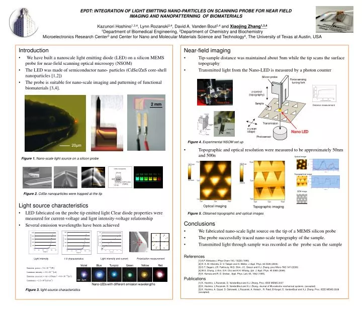
Trapped Nano-particles CdSe nanoparticle EPDT: INTEGRATION OF LIGHT EMITTING NANO-PARTICLES ON SCANNING PROBE FOR NEAR FIELD IMAGING AND NANOPATTERNING OF BIOMATERIALS Kazunori Hoshino1,3,4, Lynn Rozanski2,4, David A. Vanden Bout2,4 and Xiaojing Zhang1,3,4 1Department of Biomedical Engineering, 2Department of Chemistry and Biochemistry Microelectronics Research Center3 and Center for Nano and Molecular Materials Science and Technology4, The University of Texas at Austin, USA Introduction • We have built a nanoscale light emitting diode (LED) on a silicon MEMS probe for near-field scanning optical microsopy (NSOM) • The LED was made of semiconductor nano- particles (CdSe/ZnS core-shell nanoparticles [1,2]) • The probe is suitable for nano-scale imaging and patterning of functional biomaterials [3,4]. Light source characteristics • LED fabricated on the probe tip emitted light Clear diode properties were measured for current-voltage and lignt intensity-voltage relationship • Several emission wavelengths have been achieved Near-field imaging • Tip-sample distance was maintained about 5nm while the tip scans the surface topography • Transmitted light from the Nano-LED is measured by a photon counter • Topographic and optical resolution were measured to be approximately 50nm and 500n Conclusions • We fabricated nano-scale light source on the tip of a MEMS silicon probe • The probe successfully traced nano-scale topography of the sample. • Transmitted light through sample was recorded as the probe scan the sample References [1] A.P. Alivisatos J Phys Chem 100, 13226 (1996) [2] R. A. M. Hikmeta, D. V. Talapin and H. Weller, J. Appl. Phys. 93 3509 (2003) [3] G.T. Dagani, J.R. Fakhoury, W.G. Shin, J.C. Sisson and X.J. Zhang, proc Micro-TAS 1411(2006) [4] W.S. Chang, J. Kim, S.H. Cho and K.H. Whang, Jpn. J. Appl. Phys. 45 2083 (2006) [5] K. Karraia and R. D. Grober, Appl. Phys. Lett. 66, 1842 (1995). Publications [1] K. Hoshino, L.Rozanski, D. VandenBout and X.J. Zhang, Proc. IEEE MEMS 2007 [2] K. Hoshino, L.Rozanski, D. VandenBout and X.J. Zhang, Journal of Microelectro mechanical systems (accepted) [3] K. Hoshino, A. Gopal. D. Ostrowski, L.Rozanski, A. Heitsch , R. Patel, B Korgel, D. VandenBout and X.J. Zhang, Proc. IEEE MEMS 2008 (accepted) Distance measurement • Figure 4. Experimental NSOM set up Optical image • Figure 1. Nano-scale light source on a silicon probe Topographical image SEM image • Figure 2. CdSe nanoparticles were trapped at the tip Optical imaging Topographic imaging • Figure 5. Obtained topographic and optical images Light intensity Light intensity and current • Polarization measurement I-V characteristics • Figure 3. light-source characteristics