Download
1 / 31
320 likes | 546 Vues
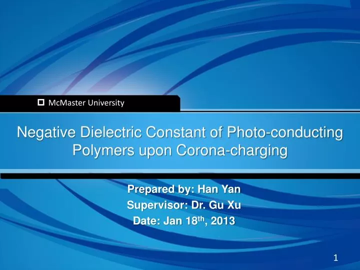
Negative Dielectric Constant of Photo-conducting Polymers upon Corona-charging. McMaster University. Prepared by: Han Yan Supervisor: Dr. Gu Xu Date: Jan 18 th , 2013. Outline. Introduction 1. Photoconductors 2. Working Principle of A Laser Printer Problem:

E N D
Negative Dielectric Constant of Photo-conducting Polymers upon Corona-charging • McMaster University Prepared by: Han Yan Supervisor: Dr. GuXu Date: Jan 18th, 2013
Outline • Introduction 1. Photoconductors 2. Working Principle of A Laser Printer • Problem: 1. The Origin of the Unwanted Surface Conduction 2. Why Significant? • Experiment Details • Results and Discussion • Three Possible Explanations • Negative Dielectric Constant (NDC) • Summary and Future Work 2
Introduction: Photoconductor • The overall hardcopy market: $80 Billion • An average of 15% annual growth • Laser printers posted the strongest growth up 25 % • Transparent polymer, electrically insulating in dark • Become hole-conductive upon illumination Drum Photoconductor Laser Light 3
Problem: The Origin of Unwanted Surface Conduction + Light Exposure + + + + + + + Dark Region Dark Region CTL: charges are transported vertically to annihilate surface charge; relatively thick. CGL: holes and electrons separated; relatively thin. Holes • It is as a result of the UNWANTED conduction ALONG the photoconductor surface, • TheDESIRABLEconduction is PERPENDICULAR to the photoconductor surface • Periphery of letter printed become fussy after repeated charges 4
Significance of The Research • A long-standing problem since 1980s, cause rapid replacement of drums • Yarmchuck (1989) and Keefe (1991) both found the blurred image was caused by surface conduction • Tokarski et al. (2007,2008) found another source of the blurred image : corona related charge accumulation in the CTL. Desirable Image Blurred Image • NO solution found, due to the unknown mechanism of photoconductor upon Corona charging 5
Experimental: Sample Preparation Spacing between electrodes ~ 1mm • Interdigitated electrode is used to maximize effective electrode area • Photoconductor: polycarbonate (PC) matrix and diphenylbenzidine (TPD) as charge transporting component Au Electrode Photoconductor Chemical Structure of TPD Portable self-made corona charger Sample is charged under high voltage for 30 mins 6
Z() M Response(X) Signal(Y) Experimental: AC Impedance Spectroscopy (IS) • To understand the origin of parallel surface conduction, ISis employed • IS: analysis of electric response of the AC perturbation, non-destructively • Analysis in frequency domain • Small perturbation I-V curve appears linear • Sine wave voltage perturbation gives sine wave current response Angular frequency: =2πf Z()=V()/ I() 7
Experimental: Step-function IS • I-t relationship is complicated: Z(t) can NOT be integrated directly • However, at any frequency ω0, Z(ω0)=V(ω0)/I(ω0) • V(t) and I(t): sum of innumerable simple harmonic oscillations at variable frequencies, after Fourier transform, V(ω) and I(ω) are obtained • Step-function ISis theoretically identical to AC IS, only technically more convenient for sample with large Time Constant Insulating material Huge Resistance τ=RC is large. Restriction in using AC: large time constant τ(extremely low resonance frequency). Low frequency IS: difficult to obtain reliable/reproducible data. Step-function IS: a step-wise potential signal, includes all frequencies on the spectrum. 8
Experimental: Step-function IS Power Supply: V(t)=0 when t<0; V(t)=U when t>=0. R V(t) C = Impedance Representation= Equivalent 9
Experimental: Measuring Device • The rising edge of the voltage source is so sharp that it is below 1 µs. A V(t) Static Charges Electrode 10
Result from Step-function IS: Current Difference Cause by Corona Charging • Figure shows the current difference as a result of surface corona charging • Fourier transform converts I(t) into frequency domain and represents it in complex form 11
Equivalent Circuit Modeling: I C R L Z’’ Z’’ Z’’ Z’ ω ω 0 . Z’ Z’ R 0 0 13
Equivalent Circuit Modeling: II . . R Z’’ Z’’ ω 0 R Z’ Z’ 0 ω 14
Equivalent Circuit Modeling: III ω ω R ω=(LC)-1/2 Z’’ Z’’ R0 R+R0 ω→0 r ω ω→∞ 0 0 ω Z’ Z’ L L R0 . . R R . . r C C 15
Result: Equivalent Circuit and Corresponding Elements Physically Unlikely Inductor winding = 0.1Henry electrosome.com 16
Similar Inductance Behavior Found in Other Areas: ion conducting polymers Roy, S.K. et al. (2007) Reversed Imaginary-axis for conventional plot Schneider, I.A. et al. (2008) Chen et al. in 2002 believed that it was a result of oxidation/reduction reaction but NO prove was given; Schneider et al. in 2008 believed that cycle of hydration and dehydration caused the unpredicted inductor BUT it was found in other systems without water hydration; Le Canut et al. in 2009 simply considered it as artefect and didn’t want to discuss further; Nanda et al. in 2011 claimed it can NOT be explained; NO explanation has been given 17
Similar Inductance Behavior Found in Other Areas: Corrosion • Cole et al. in 1941 found this mysterious inductor on a squid giant axon and gave no explanation; • Baril et al. in 1975 found this in Iron corrosion system and believed that it was as a result of Redox reaction; • Hukovic et al. found it in metal electrode anodic dissolution but he stated that the reason was “unclear”. • No explanation has been given Cole, K.S. et al. (1941) • Baril, G. et al. (2001). Reversed Imaginary-axis for conventional plot 18 • Hukovic, M.M. et al. (2002).
Survey on Possible Explanations 1 Memristor Possible Alternative Explanations 2 Quarts Crystal Resonance 3 Negative Dielectric Constant(NDC) 19
Possible Explanations 1: Memristor • Memristor was originally envisioned in 1971 by circuit theorist Leon Chua; • Recent progress reported from Nature (2008,2010), Physical Review B (2008) • It is currently under development by various teams including Hewlett-Packard for nanoelectronic memories, computer logic, and neuromorphic computer architectures • Non-linear element: impedance change as a function of voltage/current applied Strokov D.B. et al. (2008) 20
Possible Explanations 1: Memristor NO Phase Shift Voltage Source Inductor I/V Resistor Capacitor Memristor Time 0 Characteristic current curves of various circuit elements POSSIBILITY 1 IS TURNED DOWN 21
Possible Explanation 2: Quartz Crystal Resonance Piezoelectric Quartz Crystal Resonator 1cm electrosome.com POSSIBILITY 2 IS TURNED DOWN qrbiz.com Piezoelectric quartz crystal distorts when an electric field is applied; Field removed, it returns to its previous shape Energy is transformed back and forth; ElectricMechanical A non-physical inductor is found in its equivalent circuit ; Resonance frequency: ω2=1/L1C1, size dependent; Resonance frequency of sample in figures below: Mega Hertz; Resonance frequency at 1 hertz, magnitude of size: ~100 meters 22
Dielectric Polarization + + + + + + + + + + + + + + + + + + + + + + + + + + + + + + - - - - - - - - - - - - - - - - - - - - - - - - - - - - - - • Dielectrics: electrically insulating but polarizable; • NO external field: dipoles oriented randomly: electronically NEUTRAL • Polar dipoles REORIENT themselves slowly by external field; • Dipoles ALIGNED so that the internal field can CANCEL part of the external field • Dielectric constant measures how EASILY dipoles are aligned by external field: higher ɛ easy polarization 23
Dielectric Constant - - - - - - - - - - - + + + + + + + + + + + + + + + - - - - - - - - - - - - - - - - - Parallel Metal Plates Dielectric • Upon insertion, free charge on plates maintained constant: q0; • At molecular level, alignment of dipole moments inside the dielectric decrease potential over metal plates; • Total charge that contributes to the voltage: q1= q0 /ε; • Polarization(P) == Surface Density of the Polarized Charge (σ0-σ1). + + + + + + + + + + + + + 24
Dielectric Constant 25 σ0 and σ1 are the surface densities of free and total charges and they define electric displacement D and electric field E; Consequently, an application of an electric field leads to polarization. A positive dielectric constant meaning displacement is in the same direction as the applied field.
∝ Possible Explanation 3: Negative Dielectric Constant C=εA/d andε=ε*·εo ε0=Vacuum Permittivity=Constant C∝ ε Graphically in Nyquist Plot: Const* i= Turn the image 90o counter clock-wisely Z(Im) L In Impedance Result: Z(Re) +ve on Im axis R 0 -ve on Im axis C If εC<0, Zc has the same form of ZL Dielectric Constant of the Capacitor is Negative 26 Capacitors are commonly seen in the equivalent circuit for polymeric materials. Dielectric constant εfor a regular polymer is positive.
Negative Dielectric Constant Ramakrishna, S.A., (2005). • Observed were NOT inductors. They were capacitors with negative dielectric constant (NDC) • NDC stands for a induced field with OPPOSTITEdirection than the original field • Two capacitors in a circuit, one filled with a POSITIVE dielectric and the other filled with a NEGATIVEdielectric material, can become an LC resonance ω2=1/LC • If ε*of our the photoconductor is negative, we would expect a phase shift of the induced current curve to the right on the I(t)/V(t) characteristic curve for a capacitor, which isequivalent to an INDUCTOR. 27
Negative Dielectric Constant: Drude Model I Negative dielectric constant are found in plasma: Since Solve for ɛ, we have: N: Electron Density Me: Electron Mass Similar situation for metal, slightly different in the governing equation: Plasma are a ‘gas’ of free electrons. Metals are a ‘gas’ of free electrons in nuclei Assumption : electrons do not interact with each othe 28
Negative Dielectric Constant: Drude Model II Metal Plasma Dielectric constant vs normalized frequency =plasma frequency Dielectric constant is frequency dependant Free Electrons Electro-magnetic Waves 29 The plasma frequency is derived in Drude Model Conclusion 1: ω>ωp, free electron could NOT respond fast enough, wave transmitted. Conclusion 2: ω<ωp, wave mostly reflected, propagates shallow in the metal, oscillates slowly enough for the electrons to follow.
Summary and Future Work To find out the origin of surface conduction on photoconducting polymer surface that causes blurred image edge. Due to sample’s large time constant, AC IS could not obtain reliable data, step-function IS was employed. Fourier transformed step-function IS data revealed physically unlikely inductors. Negative dielectric constant in corona charged photo-conductor surface is proposed to be the explanation. To understand the nature of NDC in photoconducting polymer. To build a model for the negative dielectric constant upon corona exposure. Additionally, the understanding of NDC material at low frequency may provide possible means to make coil-less inductor. 30
Thanks for your attendance and attention Questions? 31