Hematite nanowires for solar water splitting: development and structure optimization
580 likes | 998 Vues
University of porto MAP- Fis PhD Research Conference. Hematite nanowires for solar water splitting: development and structure optimization. J. Azevedo 1,2 , C.T. Sousa 1 , M.P. Fernandez-García 1 , A. Apolinário 1 , J. M. Teixeira 1 , A.M. Mendes 2 and J.P. Araújo 1.

Hematite nanowires for solar water splitting: development and structure optimization
E N D
Presentation Transcript
University of porto MAP-Fis PhD Research Conference Hematite nanowires for solar water splitting: development and structureoptimization J. Azevedo1,2, C.T. Sousa1, M.P. Fernandez-García1, A. Apolinário1, J. M. Teixeira1, A.M. Mendes2 and J.P. Araújo1 1IN-IFIMUP and Dep. Física, Rua do Campo Alegre 687, 4169-007 Porto, Portugal 2 LEPAE – Dep. de Engenharia Quıímica, Faculdade de Engenharia, Universidade do Porto, R. Dr. Roberto Frias, 4200-465 Porto, Portugal. Porto, January 20, 2011
Outline • Introduction • Fabrication Methods • Results • Conclusions and Future work
2) Electrons (majority carriers) are conducted to a metal electrode (typically Pt) where they combine with H+ ions in the electrolyte solution to make H2 : 1) Absorption of light near the surface of the semiconductor creates electron-hole pairs. OH- OH- OH- 3) Holes (minority carriers) drift to the surface of the semiconductor (the photo anode) where they react with water to produce oxygen: 4) Transport of H+ from the anode to the cathode through the electrolyte completes the electrochemical circuit. http:/newenergyandfuel/com/2011/05/11/ O2 H2 1.23 eV Counterelectrode Photoanode + + Photoelectrochemical Cell + + +
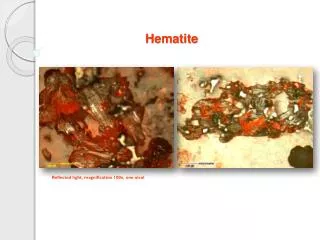
Hematite (α-Fe2O3) as photoanode Nano structuring
Pulsed Electrodeposition Pulsed Mode Pulsed deposition Barrier layer thinning Alumina Aluminium
IV V VI VII I, II III I, II III IV VI V b) a) VII VI V IV III I, II c) Perfis de Deposição
High Voltage Low Voltage 1 µm 10 µm
Atmosphere dependence on oxidation Comparison of oxidation state between different atmospheres: a) left in ambient conditions for 2 months, b) and c) annealing for 6 h at 600oC in air and oxygen, respectively. The α-Fe2O3 Bragg reflections are shown with their respective Miller indices.
Temperature dependence on oxidation Annealing temperature study on samples with 60 μm thickness. Between 400oC - 600oC the samples were annealed together with the Al substrate. For annealing’s above 600oC, the substrate was removed prior to oxidation, due to the Al melting point
Reference samples X-ray absorption spectroscopy measurements at the Fe k-edge in transmission
Higher Oxidation Lower Oxidation Comparison with prepared samples
(a), (c) and (d) SEM images of annealed NWs; (b) EDS profile of annealed NWs.
Conclusions • Fabrication of highly organized alumina templates; • Optimization of an industrially viable Fe nanowires deposition method; • Fabrication of Fe nanowires with high degree of organization with lengths from 1 μm to 10 μm up to 99 % of pore filling;
Conclusions • Enlarged nanowire surface area through pore modulation; • Oxidation studies indicate the presence of hematite after an annealing. 1 µm
Future Work • Expose only a fraction of the nanowires by a partial removal of the alumina template; • Test solar water splitting efficiencies; • Reproduce results in TiO2templates.
Thank you for your attention João Carlos Azevedo azevedo.jcam@alunos.fc.up.pt https://sites.google.com/site/azevedojcam/
O2 H2 H+ H+ H+ Potentiostat + + + + + Photoanode Counterelectrode Photoelectrochemical Scheme
Absorption of light near the surface of the semiconductor creates electron-hole pairs. Holes (minority carriers) drift to the surface of the semiconductor (the photo anode) where they react with water to produce oxygen: Electrons (majority carriers) are conducted to a metal electrode (typically Pt) where they combine with H+ ions in the electrolyte solution to make H2 : Transport of H+ from the anode to the cathode through the electrolyte completes the electrochemical circuit. The overall reaction :
Photoelectrolysis Electrolysis ElectricCurrent Photoelectrolysis Solar Cell ElectricCurrent
Nernst Equation For an oxidation/reduction reaction we have: Where F is the Faraday constant and n is the number of necessary electrons (in this case two). Energy losses
Theoretical efficiencies The overall solar energy conversion efficiency can be written as the product of the efficiencies of the cell in performing these processes:
Quais as dificuldades? • Óxidos • Quimicamente estáveis mas baixa eficiência (baixa condutividade) • Não óxidos • Boa condutividade mas fraca estabilidade química Adapted from M. Grätzel, Nature 414, 388 (2001)
Maximum efficiency possible Depending upon semiconductor bandgap, under xenon arclamp and AM1.5 solar illuminations.
Armazenamento de Hidrogénio http://en.wikipedia.org/wiki/File:XASEdges.svg • Compressed hydrogen • Liquid hydrogen • Chemical storage • Physical storage • Carbon nanotubes
First Anodization 1) 2) 3) 4) Al The four major stages of nanoporous alumina template formation: oxide barrier formation; pore initial nucleation; pore initial growth; pore continuous growth;
1 µm 1 µm Two Step Anodization 1st Anodization 2nd Anodization Dissolution of Oxide Layer Alumina Aluminium No organization Pattern formed Better organization! SEM surface
Different methods Electrodeposition different methods
Simulação numérica da influência do pulso de repouso na deposição
Influência do tamanho de poro na qualidade da deposição Amostras de 10μm de espessura, preparadas a 20oC, 0.43M e 14mA/cm2
Estrutura Cristalina • Os eletrões emitidos pelo cátodo de uma ampola onde foi previamente realizado vácuo são acelerados por um potencial elevado aplicado ao longo dela, dirigindo-se a alta velocidade em direção a uma placa metálica (alvo) utilizada como ânodo. Quando os eletrões chocam com o alvo dá-se a emissão de raios-X. • O espectro emitido é composto por radiação-X cujo comprimento de onda varia continuamente, ao qual se sobrepõe uma série de riscas muito estreitas e em posições discretas.
Estrutura Cristalina • Fatores que contribuem para o alargamento dos picos medidos experimentalmente: • tensões mecânicas não homogéneas • variações de composição ao longo da amostra • a sua espessura • as larguras e alturas das fendas de colimação do feixe (instrumento) • falta de monocromatismo do feixe incidente (instrumento) • o tamanho médio das cristalites que compõem a amostra (policristalina) • A relação entre o tamanho L e o alargamento é dada pela fórmula de Scherrer, que se escreve do seguinte modo:
// // Magnetic Characterization Coercive field: HC// (~ 1550 Oe) >> HC (~ 385 Oe) Saturation field: HS// (~ 4 kOe) << HS (~ 15 kOe)
FC and ZFC measurements ZFC and FC measurements in a 100 Oe field. The annealing temperature was 800oC. (C. H. Kim et al, “Magnetic anisotropy of vertically aligned alpha-fe2o3 nanowire array”, Ap. Phys. Let., vol. 89.)